
Page 82 - Embedded Microprocessor Systems Real World Design
P. 82
16-Bit Considerations
The interface examples shown so far have been for 8-bit processors. Interfacing
to 16-bit processors is similar except for the wider bus width. However, some 16-bit
and wider processors require somewhat more complex interfacing since they can
execute both 8- and 16-bit cycles.
The 80186 has a 16-bit bus, but if a word-wide (16-bit) memory access is per-
formed to an odd address, the processor will perform two back-to-back &bit cycles
to access the word. This is important because the processor expects to operate on
only 8 bits at a time; the remaining 8 bits are unused. Say that memory location
0006 contains the value 1B2C. The CPU may access this as a 16-bit value or it may
access either the high (1B) or low (2C) bytes. The CPU can write the lower byte to
3D, leaving the result 1B3D.
Two signals (A0 and BHE) on the 80186 control which byte of memory or 1/0
is accessed (low, high, or both). If the odd-address example happens to be a write
and the memory design assumes that all accesses will be 16 bits wide, each of the
two 8-bit writes will write invalid data to 1 byte of the memory word. The memory
logic must decode the BHE and A0 signals to determine whether just 1 byte is being
written. In the example just given, if the logic does not properly decode the A0 and
BHE signals, writing 3D to the least significant byte of the word will result in xx3D
instead of 1B3D. The xx is an unknown value-the most significant byte will be
whatever data is on the bus when the write occurs.
Other processors have similar characteristics. The 386EX is a 32-bit processor
with a 16-bit external bus, but it also can perform 8-bit cycles. When designing with
a processor that has 16 (or more) bits and can perform byte-oriented cycles, be
sure the memory design handles these operations correctly. If you are using 2-byte-
wide ICs to implement a 16-bit-wide memory, you can gate the write signal to each
memory IC with the appropriate byte select signal. On the 80186, BHE would be
used to gate the most significant byte, and A0 would be used to gate the least sig-
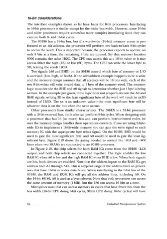
nificant byte. Figure 2.19 shows the gating needed to control the -RD and -WR
lines when two SRAMs are connected to an 80186 processor.
In Figure 2.19, the chip selects for both RAM ICs come from the 80186 -LCS
output, and both chip selects are connected together. The logic enables the low
RAM IC when A0 is low and the high RAM IC when BHE is low. When both signals
are low, both devices are enabled. Note that the address inputs to the RAM ICs get
address lines A1 through A15. This is a typical usage of the address lines on proces-
sors that have 16-bit or wider data buses. When interfacing to the 8-bit bus of the
80188, the RAM and ROM ICs will get all the address lines, including AO. On
the 16-bit 80186, A0 is used as a byte selector. Note that both processors can access
the same amount of memory (1 MB), but the 186 can access 16 bits at a time.
Microprocessors that can access memory in cycles that have fewer bits than the
bus width (16-bit CPU doing &bit cycles, 32-bit CPU doing 16-bit cycles) will have
66 Embedded Microprocessor Systems