
Page 77 - Embedded Microprocessor Systems Real World Design
P. 77
.DTACK
m
68230
-DS
ADDRESS
RSl-RSS
DATA
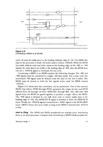
Figure 2.15
Connecting a 68230 to an 801 88.
cycle) all must be stable prior to the leading (falling) edge of -CS. The 68020 also
expects the processor to hold -CS active until it returns -DTACK. While the 80188
has stable address and read/write status at the leading edge of the -RD or -WR
signals, the write data is not stable at the leading edge of -WR. Also, the 80188 does
not use a -DTACK signal to terminate the bus cycle.
Connecting a 68230 to an 80188 requires the following changes: The -RD and
-WR signals must be converted to a single -DS data strobe. For a write cycle, the
synthesized -DS signal must be delayed until the data on the bus is stable. The
80188 must be forced to hold the bus signals active until the 68230 returns
-DTACK.
Figure 2.15 shows how this conversion can be performed. One of the internal
80188 chip selects (PCSO through PCS5) generates the range decode and 80188
address lines A0 through A4 drive 68230 RS1 through RS4. The -RD and -WR
signals from the 80188 are gated together to produce a single -DS to the 68230.
The -WR signal is delayed by one half clock cycle to ensure stable data at the
leading edge of -DS. The 80188 DT/R signal is inverted to drive the 68230 R/W
input. Finally, the -DTACK signal is returned as a -WAIT signal to the 80188 ARDY
input. ARDYis driven low (not ready) as long as the 68230 is selected and -DTACK
is false.
Intel to Zhg The 28536 and 28530 peripherals are popular parts. Interfacing
these to an Intel processor is simpler than interfacing to 68000 family peripherals.
Hardware Design 1 61