
Page 111 - Engineering Digital Design
P. 111
82 CHAPTER 3 / BACKGROUND FOR DIGITAL DESIGN
which represent LOAD and COUNT, respectively, are meaningful abbreviations called
mnemonics.
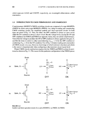
3.3 INTRODUCTION TO CMOS TERMINOLOGY AND SYMBOLOGY
Complementary MOSFET (CMOS) switching circuits are composed of n-type MOSFETs
(NMOS for short) and p-type MOSFETs (PMOS). As a help in reading and constructing
CMOS switching circuits, the simplified symbols and ideal equivalent circuits for both
types are given in Fig. 3.4. Thus, for either, the OFF condition is always an open circuit
while the ON condition is always a short circuit. But the voltage levels causing the ON and
OFF conditions for NMOS and PMOS are opposite; hence, they are called complementary.
Notice that the voltage to produce the ON or OFF condition is always applied to the gate, G,
and that the drain-to-source is either nonconducting (lorain = 0) for the OFF condition or
conducting (V DS = 0) for the ON condition. Use of Fig. 3.4 makes reading and construction
of CMOS circuits very easy. However, knowledge of which terminal is the drain and which
is the source is important only when configuring at the transistor circuit layout level.
Proper CMOS circuit construction requires that the NMOS and PMOS sections be posi-
tioned as shown in Fig. 3.5. The reason for this particular configuration is that NMOS passes
Drain
D D D
D ~ u
,A Short Circuit
(a) Gate, G — LV —• K£" HV v DS =
Circuit
I
s s s
Source
OFF ON
D
0 \ Short Circuit
Gate, G -d I HV —. LV
"J VDS " °
S S
OFF ON
FIGURE 3.4
Symbols and ideal equivalent circuits for n and p MOSFETs: (a) NMOS. (b) PMOS.