
Page 113 - Engineering Digital Design
P. 113
84 CHAPTER 3 / BACKGROUND FOR DIGITAL DESIGN
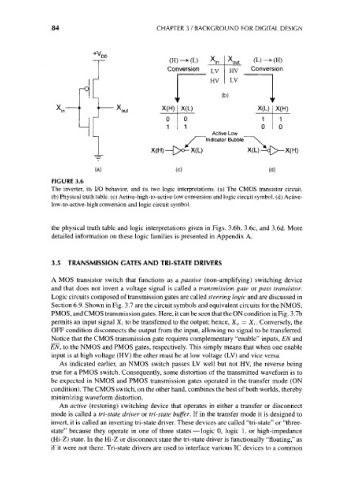
X
out
Conversion j_jy Conversion
HV LV
(b)
X X(H) X(L) X(L) X(H)
in
0 0 1
1 1 0
Active Low
Indicator Bubble \
_ X(L)A{>-X(H)
(a) (c) (d)
FIGURE 3.6
The inverter, its I/O behavior, and its two logic interpretations, (a) The CMOS transistor circuit,
(b) Physical truth table, (c) Active-high-to-active-low conversion and logic circuit symbol, (d) Active-
low-to-active-high conversion and logic circuit symbol.
the physical truth table and logic interpretations given in Figs. 3.6b, 3.6c, and 3.6d. More
detailed information on these logic families is presented in Appendix A.
3.5 TRANSMISSION GATES AND TRI-STATE DRIVERS
A MOS transistor switch that functions as a passive (non-amplifying) switching device
and that does not invert a voltage signal is called a transmission gate or pass transistor.
Logic circuits composed of transmission gates are called steering logic and are discussed in
Section 6.9. Shown in Fig. 3.7 are the circuit symbols and equivalent circuits for the NMOS,
PMOS, and CMOS transmission gates. Here, it can be seen that the ON condition in Fig. 3.7b
permits an input signal Xj to be transferred to the output; hence, X 0 = X/. Conversely, the
OFF condition disconnects the output from the input, allowing no signal to be transferred.
Notice that the CMOS transmission gate requires complementary "enable" inputs, EN and
EN, to the NMOS and PMOS gates, respectively. This simply means that when one enable
input is at high voltage (HV) the other must be at low voltage (LV) and vice versa.
As indicated earlier, an NMOS switch passes LV well but not HV, the reverse being
true for a PMOS switch. Consequently, some distortion of the transmitted waveform is to
be expected in NMOS and PMOS transmission gates operated in the transfer mode (ON
condition). The CMOS switch, on the other hand, combines the best of both worlds, thereby
minimizing waveform distortion.
An active (restoring) switching device that operates in either a transfer or disconnect
mode is called a tri-state driver or tri-state buffer. If in the transfer mode it is designed to
invert, it is called an inverting tri-state driver. These devices are called "tri-state" or "three-
state" because they operate in one of three states — logic 0, logic 1, or high-impedance
(Hi-Z) state. In the Hi-Z or disconnect state the tri-state driver is functionally "floating," as
if it were not there. Tri-state drivers are used to interface various 1C devices to a common