
Page 112 - Engineering Digital Design
P. 112
3.4 LOGIC LEVEL CONVERSION: THE INVERTER 83
MOS Supply
+V r
Passes HV well
Passes LV well
Ground
Symbol
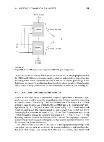
FIGURE 3.5
Proper PMOS and NMOS placement for generalized CMOS gate configurations.
LV well but not HV. Conversely, PMOS passes HV well but not LV. The proper placement of
the NMOS and PMOS sections results in a sharp, relatively undistorted waveform. Inverting
this configuration would require that the NMOS and PMOS sections pass voltage levels
that they do not pass well, resulting in a distortion of the voltage waveform. Therefore, the
PMOS section is always placed on the HV end with the NMOS on the LV side, as in Fig. 3.5.
3.4 LOGIC LEVEL CONVERSION: THE INVERTER
When a positive logic source is converted to a negative logic source, or vice versa, logic
level conversion is said to occur. The physical device that performs logic level conversion
is called the inverter. Shown in Fig. 3.6a is the CMOS version of the inverter. It is a CMOS
inverter because it is composed of both NMOS and PMOS cast in the complementary con-
figuration of Fig. 3.5. The physical truth table, shown in Fig. 3.6b, is easily understood
by referring to Fig. 3.4. The logic interpretations and conjugate logic symbols that derive
from the physical truth table are shown in Figs. 3.6c and 3.6d. The conjugate logic circuit
symbols are used to indicate the logic level conversion X(H) —>• X(L) or X(L) —>• X(H)
depending on where the active low indicator bubble is located. The designation "conjugate"
indicates that the symbols are interchangeable, as they must be since they are derived from
the same physical device (the inverter).
The CMOS inverter is used here for the purpose of developing the concept of logic level
conversion. However, there are versions of the inverter that belong to logic families other
than the CMOS family. These include the NMOS and TTL families, all of which yield