
Page 114 - Engineering Digital Design
P. 114
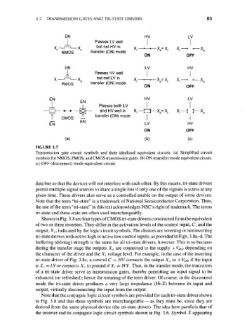
3.5 TRANSMISSION GATES AND TRI-STATE DRIVERS                          85


                             EN                               HV               LV
                             J^           Passes LV well
                         X _ i — i x      but not HV in    ^  i t x =X      X _ •  « _ X
                          1                               j
                           NMOS     °   transfer (ON) mode          o  i    i        o
                                                             ON                OFF
                                                              LV               HV
                                         Passes HV well
                                          Du  n
                                            t °t LV in   x   „  „  y _ V  Y
                                        transfer (ON) mode  '       °~ '    ]

                       EN          _ M                        HV               LV
                        i           EN
                        I            I     Passes both LV
                                 — £gj —    and HV well in  X ; — PI — X 0 =Xj  X. — I I — X 0
                            CMOS   —     transfer (ON) mode   I
                       EN          EN                        LV               HV
                                                             ON               OFF
                             (a)                              (b)              (c)

                 FIGURE 3.7
                 Transmission gate circuit symbols and their idealized equivalent circuits, (a) Simplified circuit
                 symbols for NMOS, PMOS, and CMOS transmission gates, (b) ON (transfer) mode equivalent circuit.
                 (c) OFF (disconnect) mode equivalent circuit.


                 data bus so that the devices will not interfere with each other. By this means, tri-state drivers
                 permit multiple signal sources to share a single line if only one of the signals is active at any
                 given time. These drivers also serve as a controlled enable on the output of some devices.
                 Note that the term "tri-state" is a trademark of National Semiconductor Corporation. Thus,
                 the use of the term "tri-state" in this text acknowledges NSC's right of trademark. The terms
                 tri-state and three-state are often used interchangeably.
                    Shown in Fig. 3.8 are four types of CMOS tri-state drivers constructed from the equivalent
                 of two or three inverters. They differ in the activation levels of the control input, C, and the
                 output, X 0, indicated by the logic circuit symbols. The choices are inverting or noninverting
                 tri-state drivers with active high or active low control inputs, as provided in Figs. 3.8a-d. The
                 buffering (driving) strength is the same for all tri-state drivers, however. This is so because
                 during the transfer stage the outputs X 0 are connected to the supply +VDD depending on
                 the character of the driver and the X/ voltage level. For example, in the case of the inverting
                 tri-state driver of Fig. 3.8c, a control C = HV connects the output X 0 to +VDD if the input
                 is X f = LV or connects X 0 to ground if X,• = HV. Thus, in the transfer mode, the transistors
                 of a tri-state driver serve as transmission gates, thereby permitting an input signal to be
                 enhanced (or refreshed); hence the meaning of the term driver. Of course, in the disconnect
                 mode the tri-state driver produces a very large impedance (Hi-Z) between its input and
                 output, virtually disconnecting the input from the output.
                    Note that the conjugate logic circuit symbols are provided for each tri-state driver shown
                 in Fig. 3.8 and that these symbols are interchangeable — as they must be, since they are
                 derived from the same physical device (the tri-state driver). The idea here parallels that of
                 the inverter and its conjugate logic circuit symbols shown in Fig. 3.6. Symbol X appearing