
Page 119 - Engineering Digital Design
P. 119
90 CHAPTER 3 / BACKGROUND FOR DIGITAL DESIGN
X Y Z
Logic AND LV LV HV Logic OR
Interpretation LV HV LV Interpretation
1 HV LV LV 1
1 HV HV LV 1
X(L) Y(L) Z(H) (0 > X(H) Y(H)Z(L)
1 1 1 0 0
1 0 0 0 1
0 1 0 1 0
0 0 0 1 1
X(L) • z H
; ;^i
Y L j— < ) vim-j ;°-Z(L)
Z(H) = (X-Y)(H) Z(L) = (X+Y)(L)
(a) (c) (d)
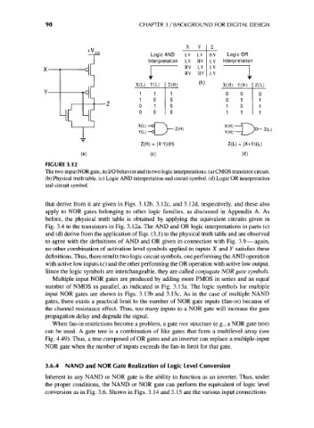
FIGURE 3.12
The two-input NOR gate, its I/O behavior and its two logic interpretations, (a) CMOS transistor circuit,
(b) Physical truth table, (c) Logic AND interpretation and circuit symbol, (d) Logic OR interpretation
and circuit symbol.
that derive from it are given in Figs. 3.12b, 3.12c, and 3.12d, respectively, and these also
apply to NOR gates belonging to other logic families, as discussed in Appendix A. As
before, the physical truth table is obtained by applying the equivalent circuits given in
Fig. 3.4 to the transistors in Fig. 3.12a. The AND and OR logic interpretations in parts (c)
and (d) derive from the application of Eqs. (3.1) to the physical truth table and are observed
to agree with the definitions of AND and OR given in connection with Fig. 3.9 — again,
no other combination of activation level symbols applied to inputs X and Y satisfies these
definitions. Thus, there results two logic circuit symbols, one performing the AND operation
with active low inputs (c) and the other performing the OR operation with active low output.
Since the logic symbols are interchangeable, they are called conjugate NOR gate symbols.
Multiple input NOR gates are produced by adding more PMOS in series and an equal
number of NMOS in parallel, as indicated in Fig. 3.13a. The logic symbols for multiple
input NOR gates are shown in Figs. 3.13b and 3.13c. As in the case of multiple NAND
gates, there exists a practical limit to the number of NOR gate inputs (fan-in) because of
the channel resistance effect. Thus, too many inputs to a NOR gate will increase the gate
propagation delay and degrade the signal.
When fan-in restrictions become a problem, a gate tree structure (e.g., a NOR gate tree)
can be used. A gate tree is a combination of like gates that form a multilevel array (see
Fig. 4.49). Thus, a tree composed of OR gates and an inverter can replace a multiple-input
NOR gate when the number of inputs exceeds the fan-in limit for that gate.
3.6.4 NAND and NOR Gate Realization of Logic Level Conversion
Inherent in any NAND or NOR gate is the ability to function as an inverter. Thus, under
the proper conditions, the NAND or NOR gate can perform the equivalent of logic level
conversion as in Fig. 3.6. Shown in Figs. 3.14 and 3.15 are the various input connections