
Page 122 - Engineering Digital Design
P. 122
3.6 AND AND OR OPERATORS AND THEIR MIXED-LOGIC CIRCUIT SYMBOLOGY 93
X Y Z T Z
Logic AND LV LV HV LV Logic OR
Interpretation LV HV LV HV Interpretation
1 HV LV LV HV 1
1 HV HV LV HV 1
v
X(L) Y(L) Z(L) ' X(H) Y(H) Z(H)
1 1 1 0 0
1 0 0 0 1
0 1 0 1 0
0 0 0 1 1
X(L}-0
Y(L)-0
NOR INV
Z(L) = (X-Y)(L) Z(H) = (X+Y)(H)
(a) (c) (d)
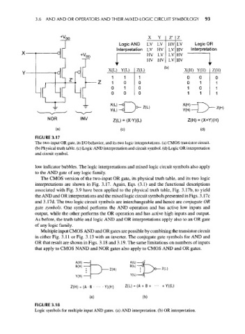
FIGURE 3.17
The two-input OR gate, its I/O behavior, and its two logic interpretations, (a) CMOS transistor circuit,
(b) Physical truth table, (c) Logic AND interpretation and circuit symbol, (d) Logic OR interpretation
and circuit symbol.
low indicator bubbles. The logic interpretations and mixed logic circuit symbols also apply
to the AND gate of any logic family.
The CMOS version of the two-input OR gate, its physical truth table, and its two logic
interpretations are shown in Fig. 3.17. Again, Eqs. (3.1) and the functional descriptions
associated with Fig. 3.9 have been applied to the physical truth table, Fig. 3.17b, to yield
the AND and OR interpretations and the mixed logic circuit symbols presented in Figs. 3.17c
and 3.17d. The two logic circuit symbols are interchangeable and hence are conjugate OR
gate symbols. One symbol performs the AND operation and has active low inputs and
output, while the other performs the OR operation and has active high inputs and output.
As before, the truth table and logic AND and OR interpretations apply also to an OR gate
of any logic family.
Multiple input CMOS AND and OR gates are possible by combining the transistor circuit
in either Fig. 3.11 or Fig. 3.13 with an inverter. The conjugate gate symbols for AND and
OR that result are shown in Figs. 3.18 and 3.19. The same limitations on numbers of inputs
that apply to CMOS NAND and NOR gates also apply to CMOS AND and OR gates.
A(H) 1 A(L) q)
B(H) \ N B(L}—$—^\ Z(L )
- -z(H) : |y°~
Y(L)—3
Y)( H) Z(L) = (A + B+ ... +Y)(L)
(b)
FIGURE 3.18
Logic symbols for multiple input AND gates, (a) AND interpretation, (b) OR interpretation.