
Page 117 - Engineering Digital Design
P. 117
88 CHAPTER 3 / BACKGROUND FOR DIGITAL DESIGN
(a) (b)
FIGURE 3.9
Distinctive logic circuit symbols for the binary operators, (a) AND symbol, (b) OR symbol.
The functional descriptions may be taken as the definitions for AND and OR. Remember
that the term active implies logic 1.
The distinctively shaped symbols in Fig. 3.9 represent the functional descriptions for
AND and OR and provide the logical interpretation for a variety of physical devices
called gates. That is, each gate must satisfy the logical AND or logical OR functional
description. By definition: A gate is an interconnection of electronic switches and other
circuit elements arranged in such a way as to produce the electrical equivalent of a logic
operation. The inputs and outputs of a gate are measured in terms of voltages (LV or
HV), whereas the inputs and outputs of a logic symbol, as in Fig. 3.9, are expressed in
terms of logic 1 or logic 0 together with the appropriate activation level indicators, (H)
and (L).
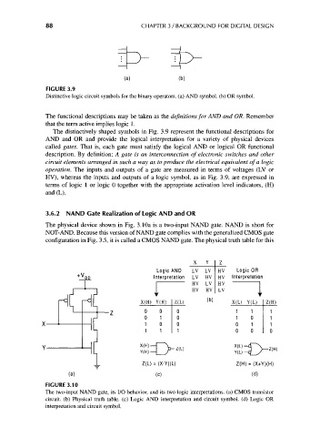
3.6.2 NAND Gate Realization of Logic AND and OR
The physical device shown in Fig. 3.10a is a two-input NAND gate. NAND is short for
NOT-AND. Because this version of NAND gate complies with the generalized CMOS gate
configuration in Fig. 3.5, it is called a CMOS NAND gate. The physical truth table for this
Logic AND LV LV HV Logic OR
Interpretation LV HV HV Interpretation
i HV LV HV i
LV
HV
HV
X(H) Y(H) Z(L) (b) X(L) Y(L) Z(H)
0 0 0 1 1 1
0 1 0 1 0 1
1 0 0 0 1 1
1 1 1 0 0 0
X(H)-
Y(H)
Z(L) = (X-Y)(L) Z(H) = (X+Y)(H)
(a) (c) (d)
FIGURE 3.10
The two-input NAND gate, its I/O behavior, and its two logic interpretations, (a) CMOS transistor
circuit, (b) Physical truth table, (c) Logic AND interpretation and circuit symbol, (d) Logic OR
interpretation and circuit symbol.