
Page 120 - Engineering Digital Design
P. 120
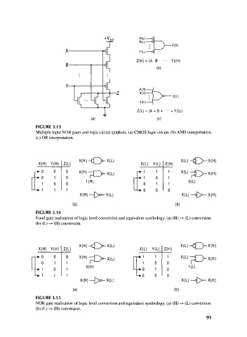
Z(H) = (A- B  Y)(H)
                                                                   (b)


                                                            A(H)-
                                                            B(H)-
                                                                         'Z(L)
                                                               • L '
                                                            Y(H)-
                                                           Z(L) = (A + B+ ••• +Y)(L)
                                                                   (c)
                  FIGURE 3.13
                 Multiple input NOR gates and logic circuit symbols, (a) CMOS logic circuit, (b) AND interpretation.
                  (c) OR interpretation.


                                                                              1
                                                                             / M -/ ^<;
                   X(H)  Y(H)  Z(L)  V  '^ — '  ^ '       X(L)   Y(L)  Z(H)
                 r* °    0    0    X(H)— f^yx(L)           r*  1  1    1     X(L)-j
                                                                                 r*
                i — * °  1    o        n —                r--+ 1  0    1
                    1    0    0                              0    1    1        0(L)
                -U- 1    1    1                            -+ 0   0    0
                                   X(H)— |>o-X(L)                            X(L)-<     X(H)
                                (a)                                       (b)
                  FIGURE 3.14
                 Nand gate realization of logic level conversion and equivalent symbology. (a) (H) —> (L) conversion.
                 (b) (L) — »• (H) conversion.


                                      ]
                   X(H) Y(H)  Z(L)  ^ ^-L^r    \ '         X (L) Y(L)  Z(H)     ^^
                                                                                 n
                IT* °    °    0    X(H}— PXx(L)            -*1    1    1 o   X(L)-H
                    0    1    1         I — ^                1    0
                --> 1    0    1     0(H)                   -*0    1    o       1 ^
                 U- 1    1    1                            U-0    0    0
                                    X(H) —[>o- X(L)                          X(L) -<P- X(H)

                                 (a)                                      (b)
                  FIGURE 3.15
                 NOR gate realization of logic level conversion and equivalent symbology. (a) (H) -»• (L) conversion,
                 (b) (L) —»• (H) conversion.
                                                                                       91