
Page 123 - Engineering Digital Design
P. 123
94 CHAPTER 3 / BACKGROUND FOR DIGITAL DESIGN
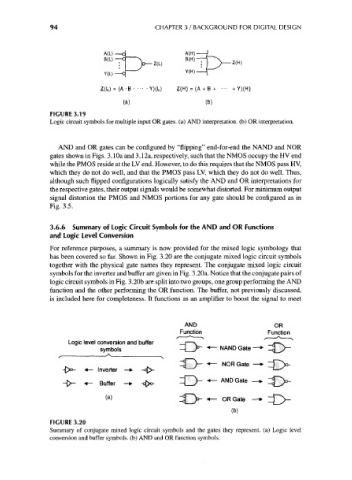
A(L) A(H)
B(L) B(H) —
'Z(L)
Y(L)
Z(L) = (A- B Y)(L) Z(H) = (A + B + ••• + Y)(H)
(a) (b)
FIGURE 3.19
Logic circuit symbols for multiple input OR gates, (a) AND interpretation, (b) OR interpretation.
AND and OR gates can be configured by "flipping" end-for-end the NAND and NOR
gates shown in Figs. 3.10a and 3.12a, respectively, such that the NMOS occupy the HV end
while the PMOS reside at the LV end. However, to do this requires that the NMOS pass HV,
which they do not do well, and that the PMOS pass LV, which they do not do well. Thus,
although such flipped configurations logically satisfy the AND and OR interpretations for
the respective gates, their output signals would be somewhat distorted. For minimum output
signal distortion the PMOS and NMOS portions for any gate should be configured as in
Fig. 3.5.
3.6.6 Summary of Logic Circuit Symbols for the AND and OR Functions
and Logic Level Conversion
For reference purposes, a summary is now provided for the mixed logic symbology that
has been covered so far. Shown in Fig. 3.20 are the conjugate mixed logic circuit symbols
together with the physical gate names they represent. The conjugate mixed logic circuit
symbols for the inverter and buffer are given in Fig. 3.20a. Notice that the conjugate pairs of
logic circuit symbols in Fig. 3.20b are split into two groups, one group performing the AND
function and the other performing the OR function. The buffer, not previously discussed,
is included here for completeness. It functions as an amplifier to boost the signal to meet
AND OR
Function Function
Logic level conversion and buffer
symbols —| }*~ *~ NAND Gate
_ , NOR Gate
-po- -4— Inverter —> -cp>-
-D>- «- Buffer -* ^>o- ILJ- ^-AND Gate
— OR Gate —*
(b)
FIGURE 3.20
Summary of conjugate mixed logic circuit symbols and the gates they represent, (a) Logic level
conversion and buffer symbols, (b) AND and OR function symbols.