
Page 127 - Engineering Digital Design
P. 127
98 CHAPTER 3 / BACKGROUND FOR DIGITAL DESIGN
(A+B+C)(L) / (A+B+C)(H)
(D+E)(L)
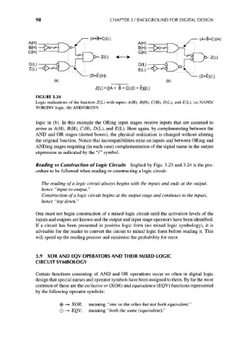
FIGURE 3.24
Logic realizations of the function Z(L) with inputs A(H), 5(H), C(H), D(L), and £(L). (a) NAND/
NOR/INV logic, (b) AND/OR/INV.
logic in (b). In this example the ORing input stages receive inputs that are assumed to
arrive as A(H), 5(H), C(H), D(L), and E(L). Here again, by complementing between the
AND and OR stages (dotted boxes), the physical realization is changed without altering
the original function. Notice that incompatibilities exist on inputs and between ORing and
ANDing stages requiring (in each case) complementation of the signal name in the output
expression as indicated by the "/" symbol.
Reading vs Construction of Logic Circuits Implied by Figs. 3.23 and 3.24 is the pro-
cedure to be followed when reading or constructing a logic circuit:
The reading of a logic circuit always begins with the inputs and ends at the output,
hence "input-to-output."
Construction of a logic circuit begins at the output stage and continues to the inputs,
hence "top down."
One must not begin construction of a mixed-logic circuit until the activation levels of the
inputs and outputs are known and the output and input stage operators have been identified.
If a circuit has been presented in positive logic form (no mixed logic symbology), it is
advisable for the reader to convert the circuit to mixed logic form before reading it. This
will speed up the reading process and minimize the probability for error.
3.9 XOR AND EQV OPERATORS AND THEIR MIXED-LOGIC
CIRCUIT SYMBOLOGY
Certain functions consisting of AND and OR operations occur so often in digital logic
design that special names and operator symbols have been assigned to them. By far the most
common of these are the exclusive or (XOR) and equivalence (EQV) functions represented
by the following operator symbols:
© —> XOR, meaning "one or the other but not both equivalent."
O —> EQV, meaning "both the same (equivalent)."