
Page 132 - Engineering Digital Design
P. 132
3.9 XOR AN D EQV OPERATORS 103
XOR gate performing the XOR gate performing the
XOR operation EQV operation
o«o <= £,:=» o-o
(a)
EQV gate performing the EQV gate performing the
XOR operation EQV operation
v
€> ^= £.. => O « O
(b)
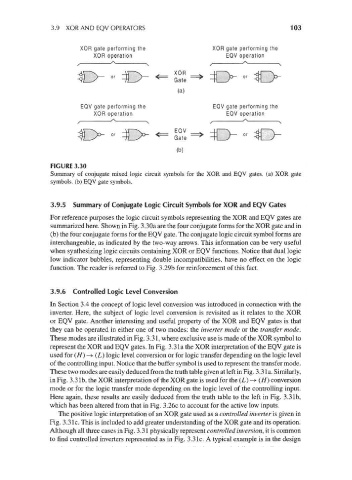
FIGURE 3.30
Summary of conjugate mixed logic circuit symbols for the XOR and EQV gates, (a) XOR gate
symbols, (b) EQV gate symbols.
3.9.5 Summary of Conjugate Logic Circuit Symbols for XOR and EQV Gates
For reference purposes the logic circuit symbols representing the XOR and EQV gates are
summarized here. Shown in Fig. 3.30a are the four conjugate forms for the XOR gate and in
(b) the four conjugate forms for the EQV gate. The conjugate logic circuit symbol forms are
interchangeable, as indicated by the two-way arrows. This information can be very useful
when synthesizing logic circuits containing XOR or EQV functions. Notice that dual logic
low indicator bubbles, representing double incompatibilities, have no effect on the logic
function. The reader is referred to Fig. 3.29b for reinforcement of this fact.
3.9.6 Controlled Logic Level Conversion
In Section 3.4 the concept of logic level conversion was introduced in connection with the
inverter. Here, the subject of logic level conversion is revisited as it relates to the XOR
or EQV gate. Another interesting and useful property of the XOR and EQV gates is that
they can be operated in either one of two modes: the inverter mode or the transfer mode.
These modes are illustrated in Fig. 3.31, where exclusive use is made of the XOR symbol to
represent the XOR and EQV gates. In Fig. 3.3 la the XOR interpretation of the EQV gate is
used for (//) —> (L) logic level conversion or for logic transfer depending on the logic level
of the controlling input. Notice that the buffer symbol is used to represent the transfer mode.
These two modes are easily deduced from the truth table given at left in Fig. 3.3 la. Similarly,
in Fig. 3.31b, the XOR interpretation of the XOR gate is used for the (L) -> (H) conversion
mode or for the logic transfer mode depending on the logic level of the controlling input.
Here again, these results are easily deduced from the truth table to the left in Fig. 3.31b,
which has been altered from that in Fig. 3.26c to account for the active low inputs.
The positive logic interpretation of an XOR gate used as a controlled inverter is given in
Fig. 3.3 Ic. This is included to add greater understanding of the XOR gate and its operation.
Although all three cases in Fig. 3.31 physically represent controlled inversion, it is common
to find controlled inverters represented as in Fig. 3.3 Ic. A typical example is in the design