
Page 133 - Engineering Digital Design
P. 133
104 CHAPTER 3 / BACKGROUND FOR DIGITAL DESIGN
X(H) Y(H) Z(L)
X(L)
0 0 = X(H) X(H) Y(H) Z(H)
0(H)
0 1
0 0
1 0
1 1 *(H)—b^X(H) 0 1
1 0
Active low output x(H) -> X(L) Transfer - I
interpretation (Inverter) (Buffer)
/ a \ Positive logic interpretation
X(L) Y(L)
*(H) 1(H) 0(H)
1 1 = X(L)
1 0 0(L) X(H)—ho-X(H) X(H)
0 1 1
0 X(L) -<f>- X(H) X(L) -<f>>- X(L) X(H) -» X(H) Transfer
^ IT (Inverter) (Buffer)
/Inom-tnrl
/Rl rff<ar\
Active low input X(L) -> X(H) Transfer
interpretation (Inverter) (Buffer)
(b) (c)
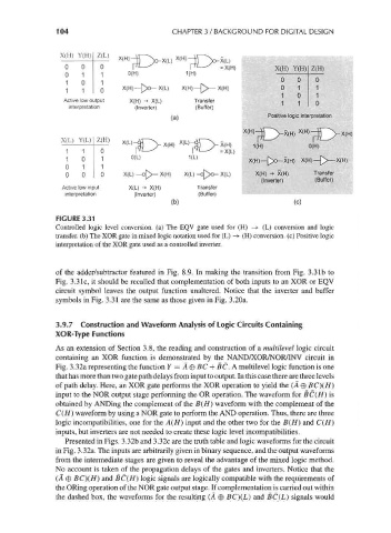
FIGURE 3.31
Controlled logic level conversion, (a) The EQV gate used for (H) —>• (L) conversion and logic
transfer, (b) The XOR gate in mixed logic notation used for (L) —>> (H) conversion, (c) Positive logic
interpretation of the XOR gate used as a controlled inverter.
of the adder/subtractor featured in Fig. 8.9. In making the transition from Fig. 3.31b to
Fig. 3.31c, it should be recalled that complementation of both inputs to an XOR or EQV
circuit symbol leaves the output function unaltered. Notice that the inverter and buffer
symbols in Fig. 3.31 are the same as those given in Fig. 3.20a.
3.9.7 Construction and Waveform Analysis of Logic Circuits Containing
XOR-Type Functions
As an extension of Section 3.8, the reading and construction of a multilevel logic circuit
containing an XOR function is demonstrated by the NAND/XOR/NOR/INV circuit in
Fig. 3.32a representing the function Y = A © BC + BC. A multilevel logic function is one
that has more than two gate path delays from input to output. In this case there are three levels
of path delay. Here, an XOR gate performs the XOR operation to yield the (A © BC)(H)
input to the NOR output stage performing the OR operation. The waveform for BC(H) is
obtained by ANDing the complement of the B(H) waveform with the complement of the
C(H) waveform by using a NOR gate to perform the AND operation. Thus, there are three
logic incompatibilities, one for the A(H) input and the other two for the B(H) and C(H}
inputs, but inverters are not needed to create these logic level incompatibilities.
Presented in Figs. 3.32b and 3.32c are the truth table and logic waveforms for the circuit
in Fig. 3.32a. The inputs are arbitrarily given in binary sequence, and the output waveforms
from the intermediate stages are given to reveal the advantage of the mixed logic method.
No account is taken of the propagation delays of the gates and inverters. Notice that the
(A © BC)(H) and BC(H) logic signals are logically compatible with the requirements of
the ORing operation of the NOR gate output stage. If complementation is carried out within
the dashed box, the waveforms for the resulting (A © BC)(L) and BC(L) signals would