
Page 134 - Engineering Digital Design
P. 134
3.10 LAWS OF BOOLEAN ALGEBRA 105
AB C
B(H)—I V (B-C)(L) 00 0
C :
<H) -LJnl^r-x(AeBC)(H) 0 0 1
0 1 0
0 1 1
1 0 0
1 0 1
(B-C)(H) i 11 0
Y = (A0BC + BC)
(c)
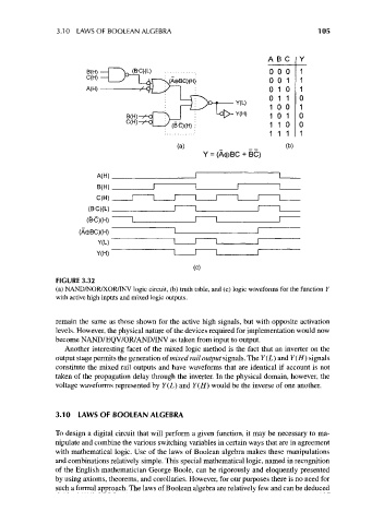
FIGURE 3.32
(a) NAND/NOR/XOR/INV logic circuit, (b) truth table, and (c) logic waveforms for the function Y
with active high inputs and mixed logic outputs.
remain the same as those shown for the active high signals, but with opposite activation
levels. However, the physical nature of the devices required for implementation would now
become NAND/EQV/OR7AND/INV as taken from input to output.
Another interesting facet of the mixed logic method is the fact that an inverter on the
output stage permits the generation of mixed rail output signals. The Y(L) and Y (H) signals
constitute the mixed rail outputs and have waveforms that are identical if account is not
taken of the propagation delay through the inverter. In the physical domain, however, the
voltage waveforms represented by Y(L) and Y(H) would be the inverse of one another.
3.10 LAWS OF BOOLEAN ALGEBRA
To design a digital circuit that will perform a given function, it may be necessary to ma-
nipulate and combine the various switching variables in certain ways that are in agreement
with mathematical logic. Use of the laws of Boolean algebra makes these manipulations
and combinations relatively simple. This special mathematical logic, named in recognition
of the English mathematician George Boole, can be rigorously and eloquently presented
by using axioms, theorems, and corollaries. However, for our purposes there is no need for
such a formal approach. The laws of Boolean algebra are relatively few and can be deduced