
Page 131 - Engineering Digital Design
P. 131
102 CHAPTER 3/BACKGROUND FOR DIGITAL DESIGN
-(A©B)(H) | ^ _ 33 )_ (A©B)(H)
L> ^ "~^
B(H)
A(H)-
U—x r^l—^Lr-x L^r-^ rL^n^-N
-(A©B)(H)
(c) (d)
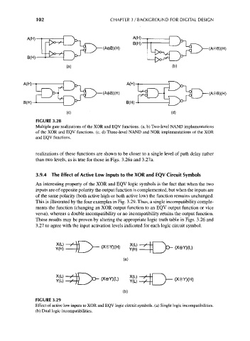
FIGURE 3.28
Multiple gate realizations of the XOR and EQV functions, (a, b) Two-level NAND implementations
of the XOR and EQV functions, (c, d) Three-level NAND and NOR implementations of the XOR
and EQV functions.
realizations of these functions are shown to be closer to a single level of path delay rather
than two levels, as is true for those in Figs. 3.26a and 3.27a.
3.9.4 The Effect of Active Low Inputs to the XOR and EQV Circuit Symbols
An interesting property of the XOR and EQV logic symbols is the fact that when the two
inputs are of opposite polarity the output function is complemented, but when the inputs are
of the same polarity (both active high or both active low) the function remains unchanged.
This is illustrated by the four examples in Fig. 3.29. Thus, a single incompatibility comple-
ments the function (changing an XOR output function to an EQV output function or vice
versa), whereas a double incompatibility or no incompatibility retains the output function.
These results may be proven by altering the appropriate logic truth table in Figs. 3.26 and
3.27 to agree with the input activation levels indicated for each logic circuit symbol.
$} ^4) j— (X0Y)(H) (X0Y)(L)
(a)
« I -**.
X(L)
Y(L) —/-U S~^ \™°' >^> Y(L) (X©Y)(H)
(b)
FIGURE 3.29
Effect of active low inputs to XOR and EQV logic circuit symbols, (a) Single logic incompatibilities,
(b) Dual logic incompatibilities.