
Page 126 - Engineering Digital Design
P. 126
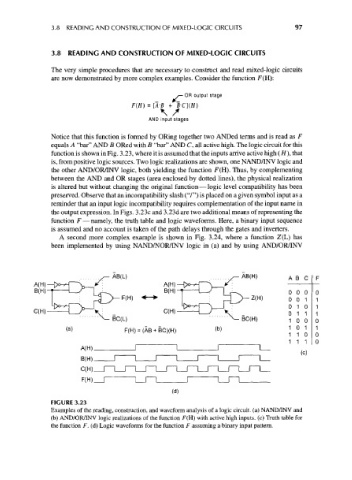
3.8 READING AND CONSTRUCTION OF MIXED-LOGIC CIRCUITS                  97


                  3.8 READING AND CONSTRUCTION OF MIXED-LOGIC CIRCUITS

                  The very simple procedures that are necessary to construct and read mixed-logic circuits
                  are now demonstrated by more complex examples. Consider the function F(H):

                                                     /— OR output stage
                                         F(H) = [A-B + B-C](H)
                                                 \ /
                                              AND input stages

                  Notice that this function is formed by ORing together two ANDed terms and is read as F
                  equals A "bar" AND B ORed with B "bar" AND C, all active high. The logic circuit for this
                  function is shown in Fig. 3.23, where it is assumed that the inputs arrive active high (//), that
                  is, from positive logic sources. Two logic realizations are shown, one NAND/INV logic and
                  the other AND/OR/INV logic, both yielding the function F(H). Thus, by complementing
                  between the AND and OR stages (area enclosed by dotted lines), the physical realization
                  is altered but without changing the original function — logic level compatibility has been
                  preserved. Observe that an incompatibility slash ("/") is placed on a given symbol input as a
                  reminder that an input logic incompatibility requires complementation of the input name in
                  the output expression. In Figs. 3.23c and 3.23d are two additional means of representing the
                  function F — namely, the truth table and logic waveforms. Here, a binary input sequence
                  is assumed and no account is taken of the path delays through the gates and inverters.
                    A second more complex example is shown in Fig. 3.24, where a function Z(L) has
                  been implemented by using NAND/NOR/INV logic in (a) and by using AND/OR/INV


                                   AB(L)                            /r-AB(H)         AB C

                                                                                     000 0
                                                                                     00 1 1
             C(H)— L^~V                           C(H) — \__J V                      011 1
                                   BC(L)                            ^BC(H)            100 0
                                                                 b
                                       F(H) = (AB + BC)(H)       ( )                  1 1 0  1
                                                                          . _ _       111 0
                                                                                         (c)


                                                    (d)
                  FIGURE 3.23
                  Examples of the reading, construction, and waveform analysis of a logic circuit, (a) NAND/INV and
                  (b) AND/OR/INV logic realizations of the function F(H) with active high inputs, (c) Truth table for
                  the function F. (d) Logic waveforms for the function F assuming a binary input pattern.