
Page 130 - Engineering Digital Design
P. 130
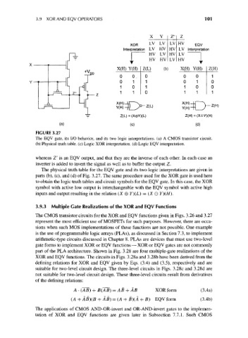
3.9 XOR AND EQV OPERATORS                                            101


                                                                X   Y   Z"  Z
                                                        XOR    LV   LV  LV  HV  EQV
                                                     Interpretation LV HV HV LV Interpretation
                                                        1      HV   LV HV LV        1
                                                                        L
                                                        1       HV HVV HV           1
                                                  X(H) Y(H)  Z(L)    (b)    X(H) Y(H)   Z(H)
                                                   0     0    0              0    0
                                                    0    1    1               0   1
                                                    1    0    1               1   0
                                                    1    1    0              1    1


                                                                                         Z(H)
                                                    Z(L) = (X®Y)(L)           Z(H) = (X©Y)(H)

                           (a)                          (C)                       (d)
                 FIGURE 3.27
                 The EQV gate, its I/O behavior, and its two logic interpretations, (a) A CMOS transistor circuit,
                 (b) Physical truth table, (c) Logic XOR interpretation, (d) Logic EQV interpretation.

                 whereas Z' is an EQV output, and that they are the inverse of each other. In each case an
                 inverter is added to invert the signal as well as to buffer the output Z.
                    The physical truth table for the EQV gate and its two logic interpretations are given in
                 parts (b), (c), and (d) of Fig. 3.27. The same procedure used for the XOR gate is used here
                 to obtain the logic truth tables and circuit symbols for the EQV gate. In this case, the XOR
                 symbol with active low output is interchangeable with the EQV symbol with active high
                 inputs and output resulting in the relation (X 0 F)(L) = (X O Y)(H).

                 3.9.3 Multiple Gate Realizations of the XOR and EQV Functions

                 The CMOS transistor circuits for the XOR and EQV functions given in Figs. 3.26 and 3.27
                 represent the most efficient use of MOSFETs for such purposes. However, there are occa-
                 sions when such MOS implementations of these functions are not possible. One example
                 is the use of programmable logic arrays (PLAs), as discussed in Section 7.3, to implement
                 arithmetic-type circuits discussed in Chapter 8. PLAs are devices that must use two-level
                 gate forms to implement XOR or EQV functions — XOR or EQV gates are not commonly
                 part of the PLA architecture. Shown in Fig. 3.28 are four multiple-gate realizations of the
                 XOR and EQV functions. The circuits in Figs. 3.28a and 3.28b have been derived from the
                 defining relations for XOR and EQV given by Eqs. (3.4) and (3.5), respectively and are
                 suitable for two-level circuit design. The three-level circuits in Figs. 3.28c and 3.28d are
                 not suitable for two-level circuit design. These three-level circuits result from derivatives
                 of the defining relations:
                                 A-(AB) + B(AB) = AB + AB         XOR form          (3.4a)

                                (A + AB)(B + AB) = (A + fi)(A + B) EQV form          (3.4b)
                 The applications of CMOS AND-OR-invert and OR-AND-invert gates to the implemen-
                 tation of XOR and EQV functions are given later in Subsection 7.7.1. Such CMOS