
Page 125 - Engineering Digital Design
P. 125
96 CHAPTER 3 / BACKGROUND FOR DIGITAL DESIGN
(X-Y)(H) + > = - ' 1 *>- (X+Y)(L)
(X-Y)(H)=(X+Y)(L)
(a) Incompatability
/ slash
Incompatibility <*YXL> = <x*Y XH)
slash (b)
FIGURE 3.21
Examples of logic level incompatibility, (a) Applications of Eqs. (3.2). (b) Use of the incompatibility
slash (/) as an alternative.
Earlier it was stated that the only logic function of the inverter is to perform logic level
conversion, (H) -> (L) or (L) —> (//), and this is true. But to what purpose? The answer
is simply stated:
The logical function of the inverter is to create or remove an input logic level incom-
patibility depending on the output function requirements of the logic symbol to which
the input is attached.
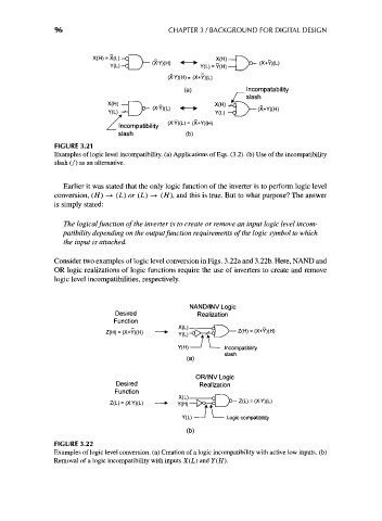
Consider two examples of logic level conversion in Figs. 3.22a and 3.22b. Here, NAND and
OR logic realizations of logic functions require the use of inverters to create and remove
logic level incompatibilities, respectively.
NAND/INV Logic
Desired Realization
Function
Z(H) = (X+Y)(H) - > Y(L)
H
Y(H) - ' < - Incompatibility
slash
(a)
OR/INV Logic
Desired Realization
Function
Z(L) = (X Y)(L)
'
n
Z(L) = (X-Y)(L) — * Y(H) — QorJI
- 1 ' -
Y(L) - 1 ' - Logic compatibility
(b)
FIGURE 3.22
Examples of logic level conversion, (a) Creation of a logic incompatibility with active low inputs, (b)
Removal of a logic incompatibility with inputs X(L) and Y(H).