
Page 121 - Engineering Digital Design
P. 121
92 CHAPTER 3 / BACKGROUND FOR DIGITAL DESIGN
that permit this to happen. These input connections result directly from the logic truth
tables in Figs. 3.10 and 3.12. The arrows on the left side of each truth table are given
to draw attention to those portions of the table that dictate how the connections to the
NAND and NOR gates must be made. For example, the extreme upper and lower arrows
in Fig. 3.14a indicate that the two inputs to the NAND gate can be connected for the
X(H ) -> Z(L) = X(L) conversion. The lower two arrows indicate that the same conversion
can be achieved by setting Y(H) = l(H). It is not likely that a NAND or NOR gate would
be used as a replacement for an inverter if the latter were available, but the substitution is
permissible if the need is there. Obviously, the NAND or NOR gate inverter is more costly
(spacewise) and is slower than the inverter in Fig. 3.6.
3.6.5 The AND and OR Gates and Their Realization of Logic AND and OR
NAND and NOR CMOS gates are natural electrical realizations of the AND and OR logic
operators, but the AND and OR CMOS gates are not. This can be understood if one recalls
that a transistor switch is, by its nature, an inverter. Thus, it might be expected that proper
CMOS realizations of NOT-AND and NOT-OR would be simpler (by transistor count) than
the equivalent CMOS realizations of AND and OR, and this is the case.
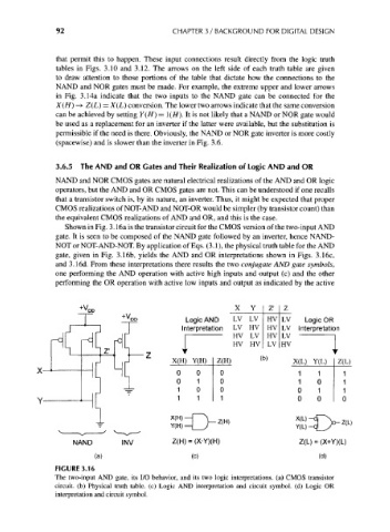
Shown in Fig. 3.16a is the transistor circuit for the CMOS version of the two-input AND
gate. It is seen to be composed of the NAND gate followed by an inverter, hence NAND-
NOT or NOT-AND-NOT. By application of Eqs. (3.1), the physical truth table for the AND
gate, given in Fig. 3.16b, yields the AND and OR interpretations shown in Figs. 3.16c,
and 3.16d. From these interpretations there results the two conjugate AND gate symbols,
one performing the AND operation with active high inputs and output (c) and the other
performing the OR operation with active low inputs and output as indicated by the active
+ X Y Z' Z
V DD
Logic AND LV LV HV LV Logic OR
Interpretation LV HV HV LV Interpretatio
H H i HV LV HV LV
HV HV
LV HV
i
^
D
X(H) Y(H) Z(H) < ' X(L) Y(L) Z(L)
x- 0 0 0 1 1
0 1 0 1 0
1 0 0 0 1
1 1 1 0 0
Y-
X(H) —
Y(H) —
NAND INV Z(H) = (XY)(H) Z(L) = (X+Y)(L)
(a) (c) (d)
FIGURE 3.16
The two-input AND gate, its I/O behavior, and its two logic interpretations, (a) CMOS transistor
circuit, (b) Physical truth table, (c) Logic AND interpretation and circuit symbol, (d) Logic OR
interpretation and circuit symbol.