
Page 124 - Engineering Digital Design
P. 124
3.7 LOGIC LEVEL INCOMPATIBILITY: COMPLEMENTATION 95
fan-in requirements. For reference purposes, the ANSI/IEEE Standard logic symbols for
gates are provided in Appendix C.I.
3.7 LOGIC LEVEL INCOMPATIBILITY: COMPLEMENTATION
The eight conjugate gate symbols in Fig. 3.20b perform one of two logic operations, AND
or OR, regardless of the presence or absence of the active low indicator bubbles that serve
to associate the symbols to the physical gates from which they are derived. However, the
presence or absence of an active low indicator bubble on the input to a given circuit symbol
indicates the activation level of the input, (L) or (H), that is "required" by that gate. Thus,
the presence of active low indicator bubbles on the inputs to a logic symbol requires that
all inputs arrive from negative logic sources while the absence of bubbles requires that the
inputs arrive from positive logic sources. When these requirements are met the inputs are
said to have logic compatibility with the logic symbol.
But suppose an input signal arrives at the input to a logic symbol with an activation level
that is of opposite polarity to that required by the logic circuit symbol. When this happens a
condition of logic incompatibility exists, and this requires that the signal name in the output
be complemented.
The operation of complementation is defined by the following important relations applied
to a logic function a:
oe(L) = d(H) and a(H) = d(L) (3.2)
such that
(a-
(a • a)(L) = 0(L)
(3.3)
The overbar is read as "the complement of." Thus, in the logic domain a logic function
a ANDed with its complement a. is logic 0, or the function ORed with its complement is
logic 1.
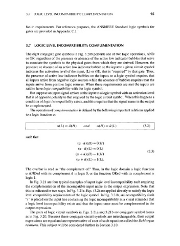
In Fig. 3.21 are four typical examples of input logic level incompatibility each requiring
the complementation of the incompatible input name in the output expression. Note that
this is indicated in two ways. In Fig. 3.21a, Eqs. (3.2) are applied directly to satisfy the logic
level compatibility requirements of the logic symbol. In Fig. 3.21b, an incompatibility slash
"/" is placed on the input line containing the logic incompatibility as a visual reminder that
a logic level incompatibility exists and that the input name must be complemented in the
output expression.
The pairs of logic circuit symbols in Figs. 3.21a and 3.21b are conjugate symbol forms
as in Fig. 3.20. Because these conjugate circuit symbols are interchangeable, their output
expressions are equal and are representative of a set of such equations called the DeMorgan
relations. This subject will be considered further in Section 3.10.