
Page 129 - Engineering Digital Design
P. 129
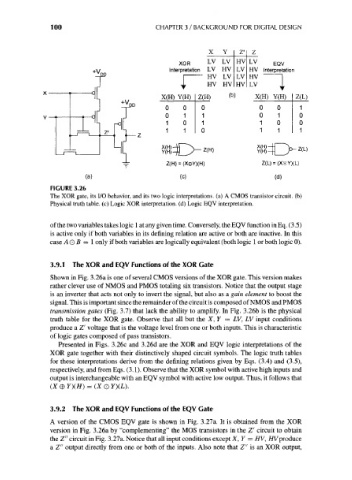
100                           CHAPTER 3 / BACKGROUND FOR DIGITAL DESIGN


                                                                 X   Y    Z'  Z
                                                         XOR     LV LV   HV  LV     EQV
                                                      Interpretation  LV HV  LV HV Interpretation
                                                                 HV LV   LV HV        I
                                                          I
                                                         I       HV HV HV LV I
                                                                        b
                                                    X(H) Y(H)  Z(H)    ( )     X(H) Y(H)  Z(L)
                                                     0    0    0                0   0
                                                     0    1    1                0    1
                                                     1    0    1                1    0
                                                     1    1    0                1    1

                                                    X(H)                                   Z(L)
                                                    Y(H)
                                                     Z{H) = (X0Y)(H)            Z(L) = (X0Y)(L)

                              (a)                        (c)                        (d)
                    FIGURE 3.26
                    The XOR gate, its I/O behavior, and its two logic interpretations, (a) A CMOS transistor circuit, (b)
                    Physical truth table, (c) Logic XOR interpretation, (d) Logic EQV interpretation.


                    of the two variables takes logic 1 at any given time. Conversely, the EQV function in Eq. (3.5)
                    is active only if both variables in its defining relation are active or both are inactive. In this
                    case A O B = 1 only if both variables are logically equivalent (both logic 1 or both logic 0).


                    3.9.1  The XOR and EQV Functions of the XOR Gate
                    Shown in Fig. 3.26a is one of several CMOS versions of the XOR gate. This version makes
                    rather clever use of NMOS and PMOS totaling six transistors. Notice that the output stage
                    is an inverter that acts not only to invert the signal, but also as a gain element to boost the
                    signal. This is important since the remainder of the circuit is composed of NMOS and PMOS
                    transmission gates (Fig. 3.7) that lack the ability to amplify. In Fig. 3.26b is the physical
                    truth table for the XOR gate. Observe that all but the X, Y = LV, LV input conditions
                    produce a Z' voltage that is the voltage level from one or both inputs. This is characteristic
                    of logic gates composed of pass transistors.
                       Presented in Figs. 3.26c and 3.26d are the XOR and EQV logic interpretations of the
                    XOR gate together with their distinctively shaped circuit symbols. The logic truth tables
                    for these interpretations derive from the defining relations given by Eqs. (3.4) and (3.5),
                    respectively, and from Eqs. (3.1). Observe that the XOR symbol with active high inputs and
                    output is interchangeable with an EQV symbol with active low output. Thus, it follows that
                    (X 0 Y)(H) = (XQ 7)(L).


                    3.9.2  The XOR and EQV Functions of the EQV Gate
                    A version of the CMOS EQV gate is shown in Fig. 3.27a. It is obtained from the XOR
                    version in Fig. 3.26a by "complementing" the MOS transistors in the Z' circuit to obtain
                    the Z" circuit in Fig. 3.27a. Notice that all input conditions except X, Y = HV, HV produce
                    a Z" output directly from one or both of the inputs. Also note that Z" is an XOR output,