
Page 118 - Engineering Digital Design
P. 118
3.6 AND AND OR OPERATORS AND THEIR MIXED-LOGIC CIRCUIT SYMBOLOGY 89
A(H)- H
B
( )—r
v Z(L)
Y(H)
Z(L) = (A- B Y)(L)
(b)
Y)(H)
(c)
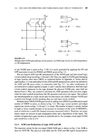
FIGURE 3.11
Multiple input NAND gates and logic circuit symbols, (a) CMOS logic circuit, (b) AND interpretation.
(c) OR interpretation.
or any NAND gate is given in Fig. 3.1 Ob. It is easily generated by applying the ON and
OFF equivalent circuits for NMOS and PMOS given in Fig. 3.4.
The two logical AND and OR interpretations of the NAND gate and their mixed logic
circuit symbols are given in Figs. 3.1 Oc and 3.1 Od. They, too, apply to NAND gates belonging
to logic families other than CMOS, as explained further in Appendix A. Notice that by
applying Eqs. (3.1) the truth tables for the AND and OR interpretations satisfy the definitions
for AND and OR given earlier in connection with Fig. 3.9 — no other combination of
activation level symbols applied to inputs X and Y satisfies these definitions. But both logic
circuit symbols represent (in the logic domain) the physical NAND gate, since both are
derived from it. Thus, one symbol (c) performs the AND operation with active low output,
while the other symbol (d) performs the OR operation with active low inputs. The symbols
are interchangeable in a logic circuit and, for that reason, are called conjugate NAND gate
symbols even though, strictly speaking, they are only logic circuit symbols.
Multiple input CMOS NAND gates result by adding more PMOS in parallel and an equal
number of NMOS in series, as shown in Fig. 3.11. The logic circuit symbols and output
expressions shown in Figs. 3.1 Ib and 3.1 Ic result. The number of inputs is usually limited
to eight or fewer, mainly because of an increase in resistance of the series N-MOSFETs,
each of which has a small ON channel resistance associated with it. Therefore, too many
inputs causes an increase in gate propagation delay and a degradation of the signal. The
number of inputs that a gate can have is called the/an-m. For example, a four-input NAND
gate would have a fan-in of 4.
3.6.3 NOR Gate Realization of Logic AND and OR
The transistor circuit for the two-input CMOS NOR gate is shown in Fig. 3.12a. NOR is
short for NOT-OR. The physical truth table and the AND and OR logical interpretations