
Page 426 - Engineering Digital Design
P. 426
396 CHAPTER 9 / PROPAGATION DELAY AND TIMING DEFECTS
Hazard cover
(B+C) fj->1 change in A
A(H)
(A+B)(L) J LT
(A+C)(L) J I
A(H)
B(H,-n 1^'\ i /
-rl ^1_
I r^ s\—*\ "-Q—N (B+C)(L)
-Y(H)
C(H) L _,, , y(H)
Small region of
(b) ' Ogic1 (c)
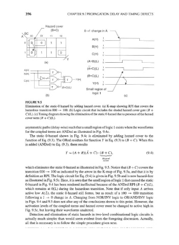
FIGURE 9.5
Elimination of the static-0 hazard by adding hazard cover, (a) K-map showing RPI that covers the
hazardous transition 000 -+ 100. (b) Logic circuit that includes the shaded hazard cover gate (B +
C)(L). (c) Timing diagram showing the elimination of the static 0-hazard due to presence of the hazard
cover term (B + C)(L).
asymmetric paths (delay-wise) such that a small region of logic 1 exists when the waveforms
for the coupled terms are ANDed as illustrated in Fig. 9.4c.
The static 0-hazard shown in Fig. 9.4c is eliminated by adding hazard cover to the
function of Eq. (9.3). The ORed residues for function Y in Eq. (9.3) is (B + C). When this
is added (ANDed) to Eq. (9.3), there results
Y = (A + B)(A + C)-(B + C), (9.4)
Hazard
cover
which eliminates the static 0-hazard as illustrated in Fig. 9.5. Notice that (B + C) covers the
transition 000 -* 100 as indicated by the arrow in the K-map of Fig. 9.5a, and that it is by
definition an RPI. The logic circuit for Eq. (9.4) is given in Fig. 9.5b and is now hazard-free
as illustrated in Fig. 9.5c. Here, it is seen that the small region of logic 1 that caused the static
0-hazard in Fig. 9.4 has been rendered ineffectual because of the ANDed RPI (B + C)(L),
which remains at 0(L) during the hazardous transition. Note that if only input A arrives
active low A(L), the static 0-hazard still forms, but as result of a 100 —*• 000 transition
following a 1 -> 0 change in A. Changing from NOR/INV logic to OR/AND/INV logic
in Figs. 9.4 and 9.5 does not alter any of the conclusions drawn to this point. However, the
activation levels of the coupled terms and hazard cover must be changed to active high in
Fig. 9.5c, but leaving their waveforms unaltered.
Detection and elimination of static hazards in two-level combinational logic circuits is
actually much simpler than would seem evident from the foregoing discussion. Actually,
all that is necessary is to follow the simple procedure given next.