
Page 423 - Engineering Digital Design
P. 423
9.2 STATIC HAZARDS IN TWO-LEVEL COMBINATIONAL LOGIC CIRCUITS 393
= gate path delay
Q1 ^ 1Q
0 0 1 )
T 3
0 1 ( V 2
h 1')
0 0
4 5 7 6
L
(a) AB < )
AC(L)
Y(H)
•Y(H) ^ Static 1-hazard
Small region of
. . %
logic 0
(b)
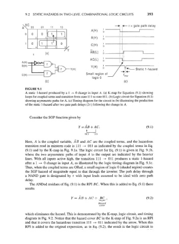
FIGURE 9.1
A static 1-hazard produced by a 1 -» 0 change in input A. (a) K-map for Equation (9.1) showing
loops for coupled terms and transition from state 111 to state 011. (b) Logic circuit for Equation (9.1)
showing asymmetric paths for A. (c) Timing diagram for the circuit in (b) illustrating the production
of the static 1-hazard after two gate path delays (2r) following the change in A.
Consider the SOP function given by
(9.1)
Here, A is the coupled variable, AB and AC are the coupled terms, and the hazardous
transition read in minterm code is 111—> Oil as indicated by the coupled terms in Eq.
(9.1) and by the K-map in Fig. 9.la. The logic circuit for Eq. (9.1) is given in Fig. 9.1b,
where the two asymmetric paths of input A to the output are indicated by the heavier
lines. With all inputs active high, the transition 111 —>• Oil produces a static 1-hazard
after a 1 -> 0 change in input A, as illustrated by the logic timing diagram in Fig. 9.1c.
Thus, when the coupled terms are ORed, a small region of logic 0 (shaded region) creates
the SOP hazard of magnitude equal to that through the inverter. The path delay through
a NAND gate is designated by r with input leads assumed to be ideal with zero path
delay.
The ANDed residues of Eq. (9.1) is the RPI BC. When this is added to Eq. (9.1) there
results
Y = AB + AC + BC , (9.2)
Hazard
cover
which eliminates the hazard. This is demonstrated by the K-map, logic circuit, and timing
diagram in Fig. 9.2. Notice that the hazard cover BC in the K-map of Fig. 9.2a is an RPI
and that it covers the hazardous transition 111 -> Oil indicated by the arrow. When this
RPI is added to the original expression, as in Eq. (9.2), the result is the logic circuit in