
Page 420 - Engineering Digital Design
P. 420
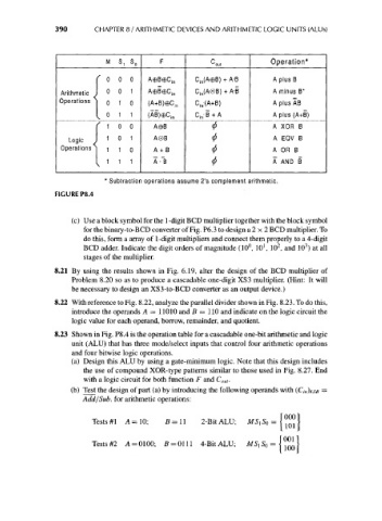
390       CHAPTER 8 / ARITHMETIC DEVICES AND ARITHMETIC LOGIC UNITS (ALUs)


                                                F                             Operation*
                                  M S 1 S 0
                                                              C out
                               {  00  0 1  0 1 0  A©B©C in  C in(A©B) + A-B   A plus B
                                  0
                                                                              A minus B*
                                                          C in (A©B) + A-B
                                             A©B©C in
                                                          C in-(A+B)
                                                                              A plus AB
                                  0
                                  0 1  1 0  1 0  (A+B)©C in  C in -B + A      A plus (A+B)
                                             (AB)©C in
                               {  1   0  1     A0B            <!>             A EQV B
                                                              (f)
                                               A©B
                                                                              A XOR B
                                      1 1
                                  1 1  1  0    A + B          * </>           A OR B
                                                                              A AND B
                                               A- B
                                  * Subtraction operations assume 2's complement arithmetic.
                     FIGURE P8.4

                         (c) Use a block symbol for the 1-digit BCD multiplier together with the block symbol
                            for the binary-to-BCD converter of Fig. P6.3 to design a 2 x 2 BCD multiplier. To
                            do this, form a array of 1-digit multipliers and connect them properly to a 4-digit
                                                                            1  2       3
                            BCD adder. Indicate the digit orders of magnitude (10°, 10 , 10 , and 10 ) at all
                            stages of the multiplier.
                     8.21 By using the results shown in Fig. 6.19, alter the design of the BCD multiplier of
                         Problem 8.20 so as to produce a cascadable one-digit XS3 multiplier. (Hint: It will
                         be necessary to design an XS3-to-BCD converter as an output device.)
                     8.22 With reference to Fig. 8.22, analyze the parallel divider shown in Fig. 8.23. To do this,
                         introduce the operands A = 11010 and 5 = 110 and indicate on the logic circuit the
                         logic value for each operand, borrow, remainder, and quotient.

                     8.23 Shown in Fig. P8.4 is the operation table for a cascadable one-bit arithmetic and logic
                         unit (ALU) that has three mode/select inputs that control four arithmetic operations
                         and four bitwise logic operations.
                         (a) Design this ALU by using a gate-minimum logic. Note that this design includes
                            the use of compound XOR-type patterns similar to those used in Fig. 8.27. End
                            with a logic circuit for both function F and C out.
                         (b) Test the design of part (a) by introducing the following operands with (Cj n)LSB —
                            Add/Sub. for arithmetic operations:

                                                                              _ f 0001
                               Tests #1 A-10;     B = ll   2-Bit ALU;  MS\S 0 =
                                                                              -jioij
                                                                                fooil
                               Tests #2 A = 0100; 5 = 0111 4-Bit ALU;  MSiS 0 =
                                                                                1100}