
Page 415 - Engineering Digital Design
P. 415
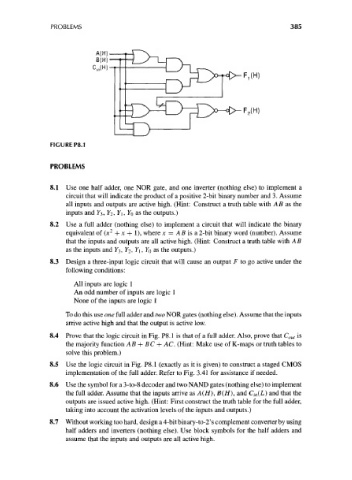
PROBLEMS                                                            385


                               A(H).
                               B(H)-
                              C, n (H)-
                                                                         F,(H)


                  FIGURE P8.1


                  PROBLEMS

                  8.1 Use one half adder, one NOR gate, and one inverter (nothing else) to implement a
                      circuit that will indicate the product of a positive 2-bit binary number and 3. Assume
                      all inputs and outputs are active high. (Hint: Construct a truth table with A B as the
                      inputs and Y^, ¥2, Y\, YQ as the outputs.)
                 8.2 Use a full adder (nothing else) to implement a circuit that will indicate the binary
                                   2
                      equivalent of (jc  4- x + 1), where x = AB is a 2-bit binary word (number). Assume
                      that the inputs and outputs are all active high. (Hint: Construct a truth table with AB
                      as the inputs and ¥3, ¥2, Y\, YQ as the outputs.)
                 8.3 Design a three-input logic circuit that will cause an output F to go active under the
                      following conditions:

                        All inputs are logic 1
                        An odd number of inputs are logic 1
                        None of the inputs are logic 1

                      To do this use one full adder and two NOR gates (nothing else). Assume that the inputs
                      arrive active high and that the output is active low.

                 8.4 Prove that the logic circuit in Fig. P8.1 is that of a full adder. Also, prove that C ou, is
                      the majority function AB + BC + AC. (Hint: Make use of K-maps or truth tables to
                      solve this problem.)
                 8.5 Use the logic circuit in Fig. P8.1 (exactly as it is given) to construct a staged CMOS
                      implementation of the full adder. Refer to Fig. 3.41 for assistance if needed.

                 8.6 Use the symbol for a 3-to-8 decoder and two NAND gates (nothing else) to implement
                      the full adder. Assume that the inputs arrive as A(H), B(H), and C in(L) and that the
                      outputs are issued active high. (Hint: First construct the truth table for the full adder,
                      taking into account the activation levels of the inputs and outputs.)
                 8.7 Without working too hard, design a 4-bit binary-to-2' s complement converter by using
                      half adders and inverters (nothing else). Use block symbols for the half adders and
                      assume that the inputs and outputs are all active high.