
Page 410 - Engineering Digital Design
P. 410
380
CGP Network of Figure £J.13
D
f5
C n t «"* o p ( \ C 2 K l "1 G! P 0 G 0 C 0
j k C3 j k g ^ k C j L
^ L L i ik
M 0, GO. ^
X
•Add/Sub
A, B \
2
" (!) 0 (Ii
G, B A G t B A G } E\ A
cj c tai ^— J
rries to 1-Bit 1-BM '" 1-Bit
OD D P' ^ ^ H'
stage PALU, „ P PALU, „ ^ PALLt o „ _ - s\
u
.4 — . ^in U ^i, ^ u ««« ^ — ^sr
^
GO RI Rfl GO H, R 0 G p ^, *0
) >
ijr J 1\ r
' r
i,)L 1 0 i r { > ir
C R t n n n P g (j C 2 P, G, G! P 0 G 0 C 0
CGP Network of Figure 8.13
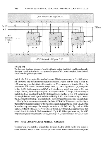
FIGURE 8.48
The three least significant bit stages of an n-bit arithmetic module for a PALU with CLA and comple-
tion signal capability showing the carry generate/propagate (CGP) network required for the dual-rail
carries and carry generate parameters.
logic 0 (Go, P'), as required for dual-rail carries. This is demonstrated in Fig. 8.48, where
for simplicity only the arithmetic module is featured. Notice that the carry-in's for the
LSB stage are properly initialized for addition or 2's complement arithmetic. Hence, for
subtraction, Add/Sub = I introduces a logic 1 into C,- n 1 and a logic 0 into C/ nO, as required
by Eq. (2.14). But for addition, Add/Sub = 0 introduces a logic 0 into carry-in C, nl and
a logic 1 into C/ nO (meaning 0 carry-in). To complete the PALU design, it is necessary to
include the logic module in Fig. 8.42 with the arithmetic module in Fig. 8.48 and combine
the completion and result signals as indicated in Fig. 8.47c. It is also necessary to connect
the Xj output from the logic module to the Bj input of the arithmetic module for each stage.
Clearly, the hardware commitment for the dual-rail CLA PALU increases considerably as
the number of stages increases. For this reason it is recommended that the group CLA method
be used on, say, 4-bit stages. For example, each of the 1-bit PALUs in Fig. 8.48 would be
replaced by four 1-bit stages of a "conventional" type (i.e., without CLA capability) and then
cascaded with the dual-rail CPG networks as in Fig. 8.48. This requires that only the MSB
stage of each group of four need be altered, as in Fig. 8.47, to accommodate the CLA feature.
8.10 VHDL DESCRIPTION OF ARITHMETIC DEVICES
To recap what was stated or intimated in Section 6.10, the VHDL model of a circuit is
called its entity, which consists of an interface description and an architectural description.