Page 406 - Engineering Digital Design
P. 406

M
                                         T/R
                                      m
                                              AHH/^uh
                         FS-FO
                              M i
 *
                                         1
 FIGURE 8.45
 «—
                           4y
      DR
          B
          A
                4
                          — H
 )
 1
                '
 Done
          F' B
 R
  1-bitPALU n1
 R
 n n-1
         j-t B J+i M i  M oGO
 in
      Add/Sub
 ^
 1
 a a a
 DONE
 n-input
 D D 0 4
 NOR gate
  _...„_
 t
 J, A
      DR
          B
  C out 1
 ^
          A
                4
 ]f
                '
 Done
         •M
  1 -bit PALU.
 R
 D 1
 r*
 •i
          F :  B *U^l ^ G0
  C in'
 '"
      Add/Sub
 ^
 « —

      DR
          B
 C out 1
 1
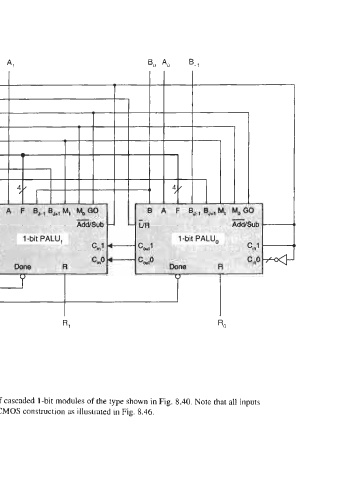
 and outputs are assumed to be active high and that the rc-input NOR gate is of CMOS construction as illustrated in Fig. 8.46.
          A
                                                    B o  A o
                4
 )f
                 /
          F :
 Done
                                                   B_,
  1-bitPALU n
 p
 „
 0
          B J-1  E J^ M t M 0 GO
 °in'
      Add/Sub
 Logic circuit for an «-bit PALU with completion signal capability consisting of cascaded 1-bit modules of the type shown in Fig. 8.40. Note that all inputs
  P 1
 c «° ^

 w
 ^
   401   402   403   404   405   406   407   408   409   410   411