Page 408 - Engineering Digital Design
P. 408
378        CHAPTER 8 / ARITHMETIC DEVICES AND ARITHMETIC LOGIC UNITS (ALUs)


                    or more of the inputs are at HV, the output is pulled low (to LV). Thus, the PMOS must be
                    specially designed so that the Drain-to-Source resistance remains sufficiently high so as to
                    minimize Drain current when one or more of the NMOS are turned ON. Here, the PMOS
                    serves the same function as the depletion-mode NMOS in Fig. A.I of Appendix A. Both
                    function as pull-up transistors. Hence, the CMOS NOR gate of Fig. 8.46 could be replaced
                    by the NMOS technology of Figure A. 1. In any case, the NOR gate logic symbol for this
                    circuit is given in Fig. 8.46b, which is the same as that in Fig. 3.13b.


                    8.9.1 Carry Look-Ahead Configuration
                    Like the R-C adder of Fig. 8.5, the PALU just described suffers a size limitation due to the
                    ripple-carry effect. The carry propagation time increases with increase in the size of the
                    PALU. To reduce significantly the propagation time, carry look-ahead (CLA) capabilities
                    can be incorporated into a dual-rail PALU design. From Eqs. (8.7) the following definitions
                    can be applied to the /th 1-bit PALU module:


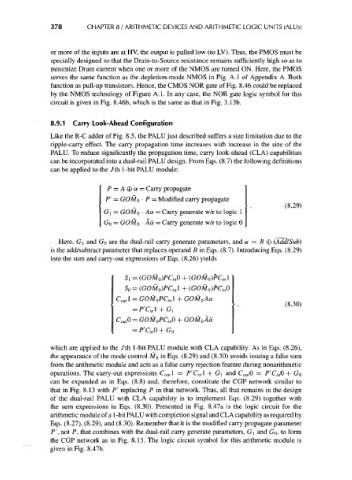
                                    P = A 0 a = Carry propagate
                                    P' = GOMo • P = Modified carry propagate
                                                                                       (8.29)
                                      = GOMo • Act = Carry generate w/r to logic 1
                                   GO = GOMo • Act = Carry generate w/r to logic 0

                       Here, G\ and GO are the dual-rail carry generate parameters, and a = B © (Add/Sub)
                    is the add/subtract parameter that replaces operand B in Eqs. (8.7). Introducing Eqs. (8.29)
                    into the sum and carry-out expressions of Eqs. (8.26) yields


                                            = (GOMo)PC inO + (GOM 0)PC in 1
                                            - (GOM 0)PC inl + (GOMo)PC inO
                                       C outl = GOMoPdn 1 + GOMoAa
                                                                                       (o.JO)

                                       C outO = GOMoPdnO + GOMoAa


                    which are applied to the /th 1-bit PALU module with CLA capability. As in Eqs. (8.26),
                    the appearance of the mode control MQ in Eqs. (8.29) and (8.30) avoids issuing a false sum
                    from the arithmetic module and acts as a false carry rejection feature during nonarithmetic
                    operations. The carry-out expressions C OM\ = P'C in\ + GI and C outO = P'C inO + GO
                    can be expanded as in Eqs. (8.8) and, therefore, constitute the CGP network similar to
                    that in Fig. 8.13 with P' replacing P in that network. Thus, all that remains in the design
                    of the dual-rail PALU with CLA capability is to implement Eqs. (8.29) together with
                    the sum expressions in Eqs. (8.30). Presented in Fig. 8.47a is the logic circuit for the
                    arithmetic module of a 1 -bit PALU with completion signal and CLA capability as required by
                    Eqs. (8.27), (8.29), and (8.30). Remember that it is the modified carry propagate parameter
                    P', not P, that combines with the dual-rail carry generate parameters, GI and GO, to form
                    the CGP network as in Fig. 8.13. The logic circuit symbol for this arithmetic module is
                    given in Fig. 8.47b.

