
Page 407 - Engineering Digital Design
P. 407
8.9 DUAL-RAIL SYSTEMS AND ALUs WITH COMPLETION SIGNALS 377
BJ+I, must be connected appropriately for left and right shifting as shown. Barrel shifting
(rotation) right can be accomplished by connecting the RQ output to the B n input. Similarly,
barrel shifting left results if the R n~\ output is connected to the B_i input. Notice that
the carry-in inputs, C inl and C, nO, to the LSB (PALU 0) stage are correctly initialized
for add or 2's complement arithmetic (see Subsection 8.3.1 regarding adder/subtractors).
Thus, if Add/Sub = 1, required for subtraction by 2's complement, a logic 1 is carried in to
the LSB stage (C in\ = 1). Conversely, if Add/Sub = 0 for addition, a logic 0 is carried in
(Cft,0=l).
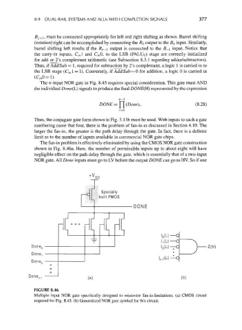
The n-input NOR gate in Fig. 8.45 requires special consideration. This gate must AND
the individual Done(L) signals to produce the final DONE(H) represented by the expression
n-\
DONE = Y\ (Done)i. (8.28)
i=Q
Thus, the conjugate gate form shown in Fig. 3.13b must be used. With inputs to such a gate
numbering more that four, there is the problem of fan-in as discussed in Section 4.10. The
larger the fan-in, the greater is the path delay through the gate. In fact, there is a definite
limit as to the number of inputs available in commercial NOR gate chips.
The fan-in problem is effectively eliminated by using the CMOS NOR gate construction
shown in Fig. 8.46a. Here, the number of permissible inputs up to about eight will have
negligible effect on the path delay through the gate, which is essentially that of a two-input
NOR gate. All Done inputs must go to LV before the output DONE can go to HV. So if one
Specially
built PMOS
DONE
H(-H H(H(
Done 0
Done,
Done 2
D ne (a) (b)
° n-1
FIGURE 8.46
Multiple input NOR gate specifically designed to minimize fan-in-limitations. (a) CMOS circuit
required for Fig. 8.45. (b) Generalized NOR gate symbol for this circuit.