
Page 401 - Engineering Digital Design
P. 401
372 CHAPTER 8 / ARITHMETIC DEVICES AND ARITHMETIC LOGIC UNITS (ALUs)
X
M 1 M 0 J
0 0 J
I Logic M\° 0 1
\M n
p I operations
0 1
J s 0 ( FJ FJ
1 0 OR*,, U/R.B , 1
J4
+
L/H*tJ » 4 + L/R'Bi,4 UR'Bj., t L/R-Bj., )
t J- * J-r (
1 1 L/R-Bj., + L/R-B J+1
(a) (b)
Xj L TO
0 0 G0-M 0
1 GO-M O 0
(c)
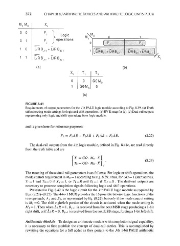
FIGURE 8.41
Requirements of output parameters for the 7th PALU logic module according to Fig. 8.39. (a) Truth
table showing mode settings for logic and shift operations, (b) EV K-map for (a), (c) Dual-rail outputs
representing only logic and shift operations from logic module.
and is given here for reference purposes:
Fj = F 3AB + F 2AB + F ]AB + F 0AB. (8.22)
The dual-rail outputs from the Jth logic module, defined in Fig. 8.41c, are read directly
from the truth table and are
f r, = GO • MQ • X ]
{ -\ (8-23)
The meaning of these dual-rail parameters is as follows: For logic or shift operations, the
mode control requirement is M 0 = 1 according to Fig. 8.39. Thus, for GO = 1 (start active),
TI = I and TQ = 0 if Xj = 1, or T\ = 0 and T 0 = 1 if Xj = 0 . The dual-rail outputs are
necessary to generate completion signals following logic and shift operations.
Presented in Fig. 8.42 is the logic circuit for the 7th PALU logic module as required by
Eqs. (8.21)-(8.23). The 4-to-l MUX provides the 16 possible bitwise logic functions of the
two operands, Aj and Bj, as represented by Eq. (8.22), but only if the mode control setting
is MI = 0. The shift right/left portion of the circuit is activated when the mode setting is
M\ = 1. Then when L/R = 1, Bj +\ is received from the next MSB stage producing a 1-bit
right shift, or if L/R = 0, Bj-\ is received from the next LSB stage, forcing a 1-bit left shift.
Arithmetic Module To design an arithmetic module with completion signal capability,
it is necessary to first establish the concept of dual-rail carries. This is accomplished by
rewriting the equations for a full adder as they pertain to the 7th 1-bit PALU arithmetic