
Page 525 - Engineering Digital Design
P. 525
11.2 DETECTION AND ELIMINATION OF OUTPUT RACE GLITCHES 495
D A = AX + B D B = AX + BX
(a) (b)
X(H)-
Y(H)
4 /
- D Q
A
p> Q 0—
L •>
, ^_ j
B(H) ^ - D Q
B \ \ —
-> Q o — v
Next state logic Output logic
CK
(c)
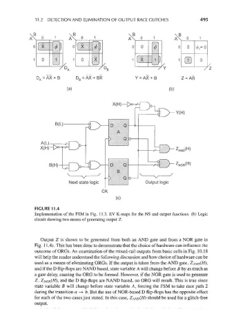
FIGURE 11.4
Implementation of the FSM in Fig. 11.3. EV K-maps for the NS and output functions, (b) Logic
circuit showing two means of generating output Z.
Output Z is shown to be generated from both an AND gate and from a NOR gate in
Fig. 11.4c. This has been done to demonstrate that the choice of hardware can influence the
outcome of ORGs. An examination of the mixed-rail outputs from basic cells in Fig. 10.18
will help the reader understand the following discussion and how choice of hardware can be
used as a means of eliminating ORGs. If the output is taken from the AND gate, ZA/VD(^),
and if the D flip-flops are NAND based, state variable A will change before B by as much as
a gate delay, causing the ORG to be formed. However, if the NOR gate is used to generate
Z, Z NOR(H), and the D flip-flops are NAND based, no ORG will result. This is true since
state variable B will change before state variable A, forcing the FSM to take race path 2
during the transition a ->• b. But the use of NOR-based D flip-flops has the opposite effect
for each of the two cases just stated. In this case, ZAND(H) should be used for a glitch-free
output.