
Page 527 - Engineering Digital Design
P. 527
11.2 DETECTION AND ELIMINATION OF OUTPUT RACE GLITCHES 497
Race path 1.. -^No ORG
.-. . - v Destination
°' gn -- X X A" State
State
Race path 2
Choice in use of don't care ^ 3
with no ORG
(a) (b)
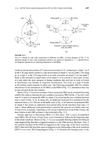
FIGURE 11.5
Use of a change in state code assignment to eliminate an ORG. (a) State diagram of Fig. 11.3a,
showing change in state code assignment and new race paths for transition b -»• c (dashed lines),
(b) Diagram segment for (a) showing elimination of all ORGs.
results in normal deactivation of Y and normal activation of Z. Assigning 03 a logic 1 or X
in the Y K-map merely results in a late deactivation of output Y via race path 2. Or, using
03 as a logic 1 in the Z K-map results in an early activation of output Z via race path 2.
Early or late activation or deactivation of an output is of no concern in most cases. In fact,
it is only under the most stringent of timing conditions that such late or early activation
or deactivation may become an important consideration. Use of 03 as a logic 0 results
in the normal output response in either case. The following paragraphs offer two simpler
alternatives for the elimination of all ORGs in the FSM of Fig. 11.3, alternatives that may
or may not provide the best solution.
Shown in Fig. 11.6 are two examples of how a potential ORG can be eliminated by using
a buffer (fly) state to eliminate the race condition causing the ORG. In Fig. 11.6a, don't-care
state 01 is used to eliminate the ORG in output Z by removing the race condition between
state a and b in Fig. 11.3a. In doing this, an additional clock period is introduced for the
transition from a to b. The use of the buffer state in Fig. 11.6b removes the potential ORG
in output Y but creates an additional clock period delay for the transition from state c to
state a. These additional clock period delays caused by the presence of a buffer state may
or may not be acceptable, depending on the design requirements for the FSM. Clearly, the
best solution to this ORG problem is that indicated in Fig. 11.5.
Another approach to eliminating ORGs is to filter them. This is easily accomplished
since ORGs, like all forms of logic noise, occur immediately following the triggering edge
of the clock waveform. Shown in Fig. II.la is an acceptable filtering scheme involving an
edge-triggered flip-flop that is triggered antiphase to the FSM memory flip-flops. Thus, if
the memory flip-flops of the FSM are triggered on the rising edge of the clock waveform
(RET), then the D flip-flop filter must be triggered on the falling edge of the clock waveform
(FET) or vice versa. The timing diagram in Fig. 11.7b illustrates the filtering action of the