
Page 134 - High Power Laser Handbook
P. 134
104 Diode Lasers Semiconductor Laser Diodes 105
The second attribute is the lasing wavelength. Here we focus on
the commercially important 800 to 1000-nm band. The 808-nm laser
has been the most widely used pump for Nd:YAG (yttrium alumi-
num garnet)-based solid-state lasers. More recently, 915-nm, 940-nm,
and 976-nm lasers have been strongly growing due to their applica-
tion in Er and Yb fiber laser and amplifier pumping and in Yb:YAG
disk laser pumping.
A third attribute is the electrical-to-optical power conversion effi-
ciency (PCE). Tremendous advances in PCE have occurred in the past
several years, with hero results in the mid-70 percent range and com-
mercial values in the mid-60 percent range.
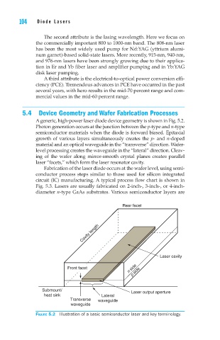
5.4 Device Geometry and Wafer Fabrication Processes
A generic, high-power laser diode device geometry is shown in Fig. 5.2.
Photon generation occurs at the junction between the p-type and n-type
semiconductor materials when the diode is forward biased. Epitaxial
growth of various layers simultaneously creates the p- and n-doped
material and an optical waveguide in the “transverse” direction. Wafer-
level processing creates the waveguide in the “lateral” direction. Cleav-
ing of the wafer along mirror-smooth crystal planes creates parallel
laser “facets,” which form the laser resonator cavity.
Fabrication of the laser diode occurs at the wafer level, using semi-
conductor process steps similar to those used for silicon integrated
circuit (IC) manufacturing. A typical process flow chart is shown in
Fig. 5.3. Lasers are usually fabricated on 2-inch-, 3-inch-, or 4-inch-
diameter n-type GaAs substrates. Various semiconductor layers are
Rear facet
Cavity length
Laser cavity
n side
Front facet
p side
Submount/ Laser output aperture
heat sink Lateral
Transverse waveguide
waveguide
Figure 5.2 Illustration of a basic semiconductor laser and key terminology.