
Page 136 - High Power Laser Handbook
P. 136
106 Diode Lasers Semiconductor Laser Diodes 107
Finally, the formation of the lateral waveguide is critical for high-
brightness, low-numerical aperture (NA) output for multimode lasers
and for kink-free operation of single-mode devices (see Sec. 5.9).
5.5 Vertical and Lateral Confinement Laser
Diode Structures
Semiconductor lasers convert electrical current into electrons and
holes that recombine at the diode junction to generate photons. For
efficient operation, the optical mode and the injected carriers must be
collocated and confined in space. Carriers are typically confined in
one or more quantum wells (QWs). The QW thickness is approxi-
mately 10 nm or less and cannot confine light, because the wave-
length is much larger than the QW thickness. To confine light, a
vertical waveguide layer is sandwiched between clad layers with a
lower refractive index. A sketch of this separate confinement hetero-
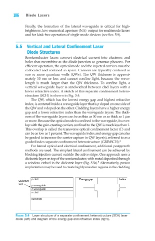
structure (SCH) is shown in Fig. 5.4.
The QW, which has the lowest energy gap and highest refractive
index, is centered inside a waveguide layer that is p doped on one side of
the QW and n doped on the other. Cladding layers have a higher energy
gap and a lower refractive index than the waveguide layers. The thick-
ness of the waveguide layers can be as thin as 50 nm or as thick as 1 mm
or more. Because the optical mode is confined to the waveguide, its over-
lap with the gain-creating carriers confined to the QW is much less than 1.
This overlap is called the transverse optical confinement factor (G) and
can be as low as 1 percent. The waveguide index and energy gap can also
be graded to increase the carrier capture in QW layer(s), referred to as a
graded index separate confinement heterostructure (GRINSCH).
4
For lateral optical and electrical confinement, additional postgrowth
methods are used. The simplest lateral confinement can be achieved by
blocking injection current outside the active stripe. One approach uses a
dielectric layer on top of the semiconductor, with metal deposited through
5
a window etched in the dielectric layer (Fig. 5.5a). Alternatively, proton
implantation may be used to create highly resistive regions in the cladding
p clad Energy gap Index
Quantum
well
p waveguide
n waveguide
n clad
substrate
Figure 5.4 Layer structure of a separate confinement heterostructure (SCH) laser
diode (left) and diagram of the energy gap and refractive index (right).