
Page 135 - High Power Laser Handbook
P. 135
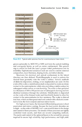
104   Diode Lasers                             Semiconductor Laser Diodes    105


                         n-type GaAs substrate
                            Epitaxial growth

                         Epitaxial characterization  3-inch wafer
                                                   (2~4 inch typ.)
                          Waveguide formation
                           p-side metallization

                            Wafer thinning
                                                               ~300 low-power bars
                                                                 (1 mm × 10 mm)
                          n-side metallization                       -or-
                                                               ~100 high-power bars
                           Metallization alloy                  (3–4 mm × 10 mm)
                              Bar cleave
                                                          25 laser die
                           Facet passivation            (3–4 mm × 0.4 mm)

                          Facet mirror coating
                         Dice into individual chips
                      Figure 5.3  Typical wafer process flow for a semiconductor laser diode.

                      grown epitaxially by MOCVD or MBE and form the optical cladding
                      and waveguide layers, as well as carrier confinement. This growth
                      step is critical for both the laser’s proper initial performance and its
                      reliability. Sophisticated analytical tools are used to confirm material
                      composition, layer thickness, doping levels, and defect density.
                         Structures  for  electrical  and  optical  confinement  in  the  lateral
                      direction are then defined. Photolithography is used to pattern the
                      desired  laser  geometry  onto  the  wafer’s  surface.  Various  methods
                      of dielectric deposition, etching, or ion implantation are used. On the
                      p side of the wafer, a metallization stack is deposited to create an ohmic
                      contact to the semiconductor, while also providing a stable surface for
                      subsequent solder reflow or wire bonding. The wafer is then polished
                      to a thickness of 100 to 150 mm for ease of subsequent cleaving and low
                      electrical resistance through the substrate. Metallization is deposited
                      on the n side of the thinned wafer and then briefly heated to alloy the
                      contact to the semiconductor for low resistance. The wafer is cleaved
                      into bars, which are then passivated and coated with a dielectric mate-
                      rial to form the front (output) and rear mirror facets.
                         For high-power lasers, the foremost differentiating process is facet
                      passivation and mirror coating. Because the facet power densities are
                                                    2
                      so high—on the order of 100 MW/cm —care must be taken in the design
                      and control of these processes. The details of these processes are tightly
                      controlled  trade  secrets,  and  there  are  several  competing  methods.
                      The purity and control of the epitaxial layers is the second key process
                      required to ensure high reliability, high performance, and high yield.