
Page 137 - High Power Laser Handbook
P. 137
106 Diode Lasers Semiconductor Laser Diodes 107
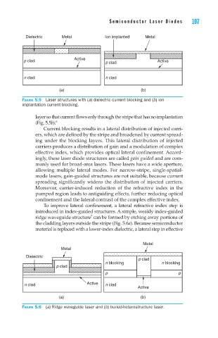
Dielectric Metal Ion implanted Metal
Active
p clad p clad Active
n clad n clad
(a) (b)
Figure 5.5 Laser structures with (a) dielectric current blocking and (b) ion
implantation current blocking.
layer so that current flows only through the stripe that has no implantation
(Fig. 5.5b). 6
Current blocking results in a lateral distribution of injected carri-
ers, which are defined by the stripe and broadened by current spread-
ing under the blocking layers. This lateral distribution of injected
carriers produces a distribution of gain and a modulation of complex
effective index, which provides optical lateral confinement. Accord-
ingly, these laser diode structures are called gain guided and are com-
monly used for broad-area lasers. These lasers have a wide aperture,
allowing multiple lateral modes. For narrow-stripe, single-spatial-
mode lasers, gain-guided structures are not suitable, because current
spreading significantly widens the distribution of injected carriers.
Moreover, carrier-induced reduction of the refractive index in the
pumped region leads to antiguiding effects, further reducing optical
confinement and the lateral contrast of the complex effective index.
To improve lateral confinement, a lateral refractive index step is
introduced in index-guided structures. A simple, weakly index-guided
7
ridge waveguide structure can be formed by etching away portions of
the cladding layers outside the stripe (Fig. 5.6a). Because semiconductor
material is replaced with a lower-index dielectric, a lateral step in effective
Metal
Metal
Dielectric
p clad
n blocking n blocking
p clad
p p
n clad Active n clad
Active
(a) (b)
Figure 5.6 (a) Ridge waveguide laser and (b) buried-heterostructure laser.