
Page 166 - High Power Laser Handbook
P. 166
134 Diode Lasers High-Power Diode Laser Arrays 135
laser bars, as well as single emitters, are assembled with the p-n junc-
tion very close (< 2 mm) to the heat sink or heat spreader (p side down).
Solder and heat sink material must be chosen carefully to avoid any
additional stress in the epitaxially grown layers, which would lead to
wavelength distortions and localized changes in polarization.
In the past, two different approaches were widely used for bar
packaging on a heat sink. The earlier process, developed in the late
1980s, was based on a soft solder (indium) and could use copper
directly as the heat-sinking material (also called direct bond). Issues
with reducing the indium surface and the interaction of indium with
the necessary gold layers (brittle InAu intermetallic) required a very
precise process control to achieve a highly reliable soft connection of
the diode laser bar with the copper heat sink. The solder had to be
soft, because the thermal expansion coefficient of GaAs and copper
are different by a factor of 3. Although substantial progress was made
addressing these packaging problems with indium, as the diode laser
materials became more and more efficient and the diode bar drive
currents reached beyond the 100-A mark, new reliability issues sur-
faced with the indium bonds. The high current density and the inter-
est in the pulsed mode of operation, where the diode bar and the soft
solder have to experience many full temperature cycles, caused the
indium bond to fail within a couple of thousand hours of operation,
due to solder migration and the well-known whisker formation.
The increased electro-optical efficiency of the diode laser materi-
als favored a second approach in which an expansion-matched mate-
rial is used to form a submount for the GaAs bar. With these
submounts, a hard solder (AuSn) can be used to package the bar.
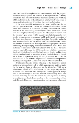
Materials like CuW have been widely used for this approach, though
with a disadvantage of reduced thermal conductivity. New sub-
mounts, including AlN and BeO materials, offer expansion matching
in combination with electrical isolation to the subsequent metal heat
sink (Fig. 6.2). These new ceramic devices work as simple submounts
Figure 6.2 Diode bar on CuW submount.