
Page 324 - Introduction to Information Optics
P. 324
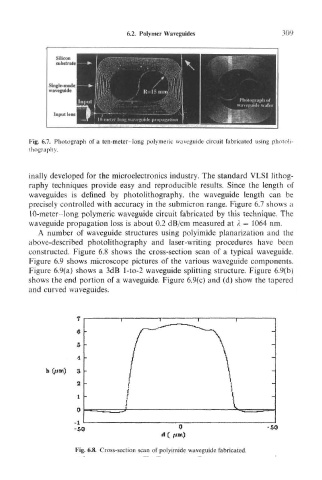
6.2. Polymer Waveguides                309


             Input


       Fig. 6.7. Photograph of a ten-meter-long polymeric waveguide circuit fabricated using photoli-
       thography.


       inally developed for the microelectronics industry. The standard VLSI lithog-
       raphy techniques provide easy and reproducible results. Since the length of
       waveguides is defined by photolithography, the waveguide length can be
       precisely controlled with accuracy in the submicron range. Figure 6.7 shows a
       10-meter-long polymeric waveguide circuit fabricated by this technique. The
       waveguide propagation loss is about 0.2 dB/cm measured at 1 = 1064 nm.
          A number of waveguide structures using polyimide planarization and the
       above-described photolithography and laser-writing procedures have been
       constructed. Figure 6.8 shows the cross-section scan of a typical waveguide.
       Figure 6.9 shows microscope pictures of the various waveguide components.
       Figure 6.9(a) shows a 3dB l-to-2 waveguide splitting structure. Figure 6,9(b)
       shows the end portion of a waveguide. Figure 6.9(c) and (d) show the tapered
       and curved waveguides.


                   4

                   3
                   2
                   1
                   a
                   -i
                   -50
                                          C
                   Fig. 6.8. Cross-section scan of polyimide waveguide fabricated.