
Page 358 - Introduction to Information Optics
P. 358
6.7. Polymer Waveguide-Based Optical Bus Structure
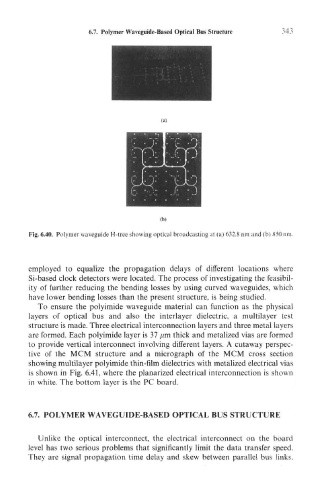
Fig. 6.40. Polymer waveguide H-tree showing optical broadcasting at (a) 632.8 nm and (b) 850 nm.
employed to equalize the propagation delays of different locations where
Si-based clock detectors were located. The process of investigating the feasibil-
ity of further reducing the bending losses by using curved waveguides, which
have lower bending losses than the present structure, is being studied.
To ensure the polyimide waveguide material can function as the physical
layers of optical bus and also the interlayer dielectric, a multilayer test
structure is made. Three electrical interconnection layers and three metal layers
are formed. Each polyimide layer is 37 /.im thick and metalized vias are formed
to provide vertical interconnect involving different layers. A cutaway perspec-
tive of the MCM structure and a micrograph of the MCM cross section
showing multilayer polyimide thin-film dielectrics with metalized electrical vias
is shown in Fig. 6.41, where the planarized electrical interconnection is shown
in white. The bottom layer is the PC board.
6.7. POLYMER WAVEGUIDE-BASED OPTICAL BUS STRUCTURE
Unlike the optical interconnect, the electrical interconnect on the board
level has two serious problems that significantly limit the data transfer speed.
They are signal propagation time delay and skew between parallel bus links.