
Page 353 - Introduction to Information Optics
P. 353
338 6. Interconnection with Optics
2. The donut-shaped mesa is rilled with SOG (Spin On Glass) to provide
low contact pad capacitance (it ensures high-frequency operation), better
planarization for metalization, and enhanced mechanical strength (help-
ful in thin VCSEL applications).
3. This step involves metalization and binding to a temporary superstrate
(sapphire). Next, the p-contact is formed by depositing a layer of
(Ti/Pt/Au), and the VCSEL is attached on a temporary sapphire super-
11
strate using Crybond" .
4. In this step the GaAs wafer is lapped till 250/tm (625 /mi —»• 250 /mi) and
back side etch holes are etched.
5. Finally, substrate is removed by introducing HF through etched hole
from backside and etching the sacrificial layer away.
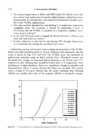
Output laser power and current versus voltage characteristics of the VCSEL
before and after polishing down to 42-/mi thickness were measured, and the
result is shown in Figs. 6.37 and 6.38. The VCSEL array was mounted on
gold-coated substrate using an InGa eutectic alloy. Threshold current and
threshold bias voltage are measured before thinning to be 5.8mA and 1.7V,
respectively, after thinning they should be 6.0mA and 1.2 V, respectively. After
polishing to its final thickness, there is no significant change in optoelectrical
characteristics. The L-I curves showed that there was no kink. The current
versus voltage (I-V) curve showed that the series resistance after thinning
(200 Q) was smaller than that of the original (300 Q) at threshold voltages.
25-
1st (thick)
20-
3rd (thick)
5th (thick)
7th (thick)
15- 9th (thick)
11st (thick)
1st (thin)
O 10- 3rd (thin)
5th (thin)
7th (thin)
9th (thin)
11st (thin)
0.5 1.0 1,5 2.0 2.5 3.0
Bias Voltage [V]
Fig. 6.37. I V characteristic of a commercially obtained VCSEL before and after thinning process