
Page 348 - Introduction to Information Optics
P. 348
6.4. Integration of Thin-Film Photodetectors 333
relatively photosensitive area of 50%. Finally, the metal pad for probing the
device was fabricated by evaporating 100 nm Cr/Au. Each photodetector
fabricated has an active area of 50 /mi x 50 /.an. Following the detector array
fabrication the polymer channel waveguide array is fabricated on the substrate-
containing photodetector array such that the active area of detectors overlaps
with the waveguide output couplers. A photograph of a portion of the
integrated system is shown in Fig. 6.32(b). Then 45° TIR micromirror couplers
are formed on each channel at the position directly above the active area of
the photodetector. Such integration facilitates precise alignment of the light
coupler with the receiver, and helps avoid difficult optical alignment and
packaging processes.
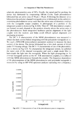
The DC I-V characteristic of the MSM photodetector was measured to
obtain the dark current before integrating with the polyamide waveguide array,
We used a HP4145B semiconductor parameter analyzer to measure the dark
current of the device. The device fabricated has a low dark current of 4.6 pA
under 5 V biasing voltage. The DC I-V characteristic of one of the photodetec-
tors is shown in Fig. 6.33. To characterize the integrated system, we polished
the input ends of the channel waveguides and used a single mode fiber to
butt-couple the light into the waveguide. When the light propagating in the
channel waveguide arrives at the 45° TIR micromirror couplers, it is reflected
onto the MSM photodetector beneath the coupler. The frequency dependence
of the photoresponse of the MSM photodetector and polyimide waveguide is
measured by using an HP 8702 spectrum analyzer operating over a frequency
0.00008 -,
0.00006 -
0.00004 -
0.00002-
0.00000-
3 -0.00002-
o
-0,00004 -
-0.00006-
-20 -10 0 10 20
Voltage(volt)
Fig. 6.33. I V characteristic of one of the photodetectors prior to integration.