
Page 347 - Introduction to Information Optics
P. 347
332 6, Interconnection with Optics
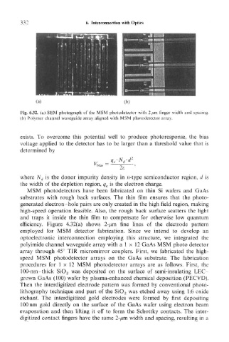
Fig. 6.32. (a) SEM photograph of the MSM photodetector with 2/an finger width and spacing.
(b) Polymer channel waveguide array aligned with MSM photodetector array.
exists. To overcome this potential well to produce photoresponse, the bias
voltage applied to the detector has to be larger than a threshold value that is
determined by
rf
y. ^^L !
bias 2g
where N d is the donor impurity density in n-type semiconductor region, d is
the width of the depletion region, q e is the electron charge.
MSM photodetectors have been fabricated on thin Si wafers and GaAs
substrates with rough back surfaces. The thin film ensures that the photo-
generated electron-hole pairs are only created in the high field region, making
high-speed operation feasible. Also, the rough back surface scatters the light
and traps it inside the thin film to compensate for otherwise low quantum
efficiency. Figure 4.32(a) shows 2-/mi fine lines of the electrode pattern
employed for MSM detector fabrication. Since we intend to develop an
optoelectronic interconnection employing this structure, we integrated the
polyimide channel waveguide array with a 1 x 12 GaAs MSM photo detector
array through 45° TIR micromirror couplers. First, we fabricated the high-
speed MSM photodetector arrays on the GaAs substrate. The fabrication
procedures for 1 x 12 MSM photodetector arrays are as follows. First, the
100-nm-thick SiO 2 was deposited on the surface of semi-insulating LEG
grown GaAs (100) wafer by plasma-enhanced chemical deposition (PECVD).
Then the interdigitized electrode pattern was formed by conventional photo-
lithography technique and part of the SiO 2 was etched away using 1:6 oxide
etch ant. The interdigitized gold electrodes were formed by first depositing
100 nm gold directly on the surface of the GaAs wafer using electron beam
evaporation and then lifting it off to form the Schottky contacts. The inter-
digitized contact fingers have the same 2-/mi width and spacing, resulting in a