
Page 342 - Introduction to Information Optics
P. 342
6.3. Thin-Film Waveguide Couplers
Photoresist A!
91200
substrate
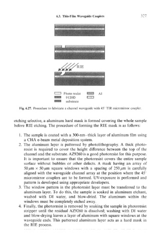
Fig. 6.27. Procedure to fabricate a channel waveguide with 45 TIR micromirror coupler.
etching selective, a aluminum hard mask is formed covering the whole sample
before RIE etching. The procedure of forming the RIE mask is as follows:
1. The sample is coated with a 300-nm-thick layer of aluminum film using
a CHA e-beam metal deposition system.
2. The aluminum layer is patterned by photolithography. A thick photo-
resist is required to cover the height difference between the top of the
channel and the substrate. AZ9260 is a good photoresist for this purpose.
It is important to ensure that the photoresist covers the entire sample
surface without bubbles or other defects. A mask having an array of
50 /mi x 50/im square windows with a spacing of 250 /mi is carefully
aligned with the waveguide channel array at the position where the 45
micromirror couplers are to be formed. UV-exposure is performed and
pattern is developed using appropriate developers.
3. The window pattern in the photoresist layer must be transferred to the
aluminum layer. To do this, the sample is soaked in aluminum etchant,
washed with DI water, and blow-dried. The aluminum within the
windows must be completely etched away.
4. Finally, the photoresist is removed by soaking the sample in photoresist
stripper until the residual AZ9260 is dissolved; washing with DI water
and blow-drying leaves a layer of aluminum with square windows at the
waveguide ends. This patterned aluminum layer acts as a hard mask in
the RIE process.