
Page 337 - Introduction to Information Optics
P. 337
322 6. Interconnection with Optics
been successfully fabricated on Si substrate by inserting a high index polyimide
layer (n — 1.56-1.76) between the 9020D cladding layers.
To form the tilted grating pattern on the polyimide waveguide, we used a
reactive ion etching (RIE) process with a low oxygen pressure of 2KPa to
transfer the grating pattern on the aluminum layer to the polyimide layer. In
order to get the tilted profile, a Faraday cage was used [21]. Microstructures
of the tilted grating having a periodicity varying from 0.5 mm to 3 mm have
been fabricated.
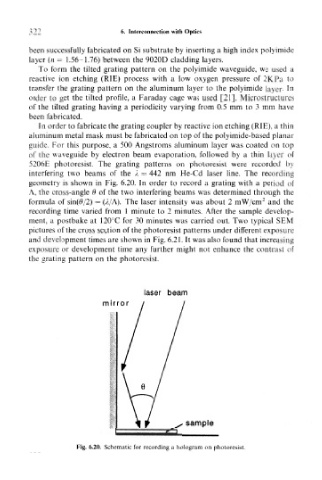
In order to fabricate the grating coupler by reactive ion etching (RIE), a thin
aluminum metal mask must be fabricated on top of the polyimide-based planar
guide. For this purpose, a 500 Angstroms aluminum layer was coated on top
of the waveguide by electron beam evaporation, followed by a thin layer of
5206E photoresist. The grating patterns on photoresist were recorded by
interfering two beams of the A = 442 nm He-Cd laser line. The recording
geometry is shown in Fig. 6.20. In order to record a grating with a period of
A, the cross-angle 6 of the two interfering beams was determined through the
2
formula of sin($/2) = (A/A). The laser intensity was about 2 mW/cm and the
recording time varied from 1 minute to 2 minutes. After the sample develop-
ment, a postbake at 120°C for 30 minutes was carried out. Two typical SEM
pictures of the cross section of the photoresist patterns under different exposure
and development times are shown in Fig. 6.21. It was also found that increasing
exposure or development time any further might not enhance the contrast of
the grating pattern on the photoresist.
laser beam
mirror
sample
Fig. 6.20. Schematic for recording a hologram on photoresist.