
Page 338 - Introduction to Information Optics
P. 338
6.3. Thin-Film Waveguide Couplers
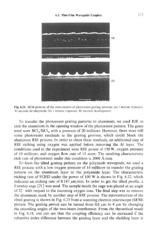
Fig. 6.21. SEM pictures of the cross section of photoresist grating patterns, (a) 1 minute exposure,
30 seconds development, (b) 1 minute exposure, 60 seconds development.
To transfer the photoresist grating patterns to aluminum, we used RLE to
etch the aluminum in the opening window of the photoresist pattern. The gases
used were BCl 3/SiCl 4 with a pressure of 20 millitorr. However, there were still
some photoresist residuals in the grating grooves, which could block the
aluminum RIE process. In order to clean these residuals, an additional step of
RIE etching using oxygen was applied before removing the Al layer. The
conditions used in the experiment were RIE power of 150 W, oxygen pressure
of 10 millitorr, and oxygen flow rate of 15 seem. The resulting characteristic
etch rate of photoresist under this condition is 2000 A/min.
To form the tilted grating pattern on the polyimide waveguide, we used a
RIE process with a low oxygen pressure of 10 millitorr to transfer the grating
pattern on the aluminum layer to the polyimide layer. The characteristic
etching rate of 9120D under the power of 100 W is shown in Fig. 6.22, which
indicates an etching rate of 0.147 ^m/min. In order to get the tilted profile, a
Faraday cage [21] was used. The sample inside the cage was placed at an angle
of 32 with respect to the incoming oxygen ions. The final step was to remove
the aluminum mask by another step of RIE process. The microstructure of the
tilted grating is shown in Fig. 6.23 from a scanning electron microscope (SEM)
picture. The grating period can be turned from 0.6 jum to 4 /im by changing
the recording angles of the two-beam interference. From the theoretical result
in Fig. 6.18, one can see that the coupling efficiency can be increased if the
refractive index difference between the guiding layer and the cladding layer is