
Page 306 - System on Package_ Miniaturization of the Entire System
P. 306
280 Cha pte r F i v e
interconnections, and microvias for achieving high-density interconnections [39]. A
maximum Q in excess of 70 was reported in the C band. The Nelco N4000-6 type is
another organic material on which planar CPW loop inductors with a high Q of 85 in
the 5-GHz range were demonstrated [40].
Another method to achieve very high Q, a maximum Q of 100 for a 3.6-nH inductor
at 1.8 GHz, involved standard FR4 substrate using a buildup layer of Dupont Vialux
material [41–42]. The process used was a low-cost process based on large-area multi-
chip module-laminated (MCM-L) technology. The self-resonance frequency was 10.6 GHz.
About 150 variations of the inductor designs were built on this testbed, and the structures
were examined for variations in parameters such as line width, spacing, ground
separation, and the number of inductor turns. Dupont Vialux also produced some very
good results for cascaded loop inductors. A Q factor of 103 was demonstrated for a, 11-nH
inductor at 2.2 GHz with a self-resonant frequency of 3.6 GHz [41]. A unique design
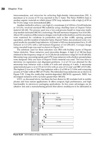
using cascaded loops was used as shown in Figure 5.19.
The substrate used for these inductors was FR4 with buildup layers of Dupont
Vialux dielectric. These inductors used microstrip designs. A high Q of 180 has been
obtained in the frequency range of 1 to 3 GHz for an inductance range of 1 to 20 nH [42].
Microstrip loop, microstrip spiral, and CPW loop inductors with a hollow ground plane
were designed. Only one layer of Dupont Vialux material was used. This was done to
minimize via registration and alignment problems. A Q of 110 was obtained for the
microstrip loop inductor with a width of 6 mils and spacing of 4 mils. A microstrip
spiral inductor gave a Q of 170 at 2.4 GHz with an area of 3.2 mm and SRF of 8.5 GHz.
2
The highest Q was for a CPW loop inductor with a Q of 180 at 2.2 GHz and occupying
2
an area of 9 mm with an SRF of 5.5 GHz. The fabricated loop inductors are as shown in
Figure 5.19. Using the multi-chip module-deposited (MCM-D) approach, IMEC has
developed inductors with a Q factor greater than 100 [43].
LTCC, as discussed above, has been the best choice for RF modules both in mobile
phones and base station applications. It offers compact, high performance, and high
functionality in microwave packaging applications. Its two main advantages are its
ultralow loss and a manufacturing process that allows multilayers to be fabricated in
Vias to metal 2 A
1 loop
240 mils
2 loop
Ground
3 loop
FIGURE 5.19 Schematics of loop inductors. [42]