
Page 305 - System on Package_ Miniaturization of the Entire System
P. 305
Radio Fr equency System-on-Package (RF SOP) 279
Via
Au (2 μm)
Polyimide
Ground
plane
Au (1 μm)
Si Substrate (625 μm, ρ = 30 cm)
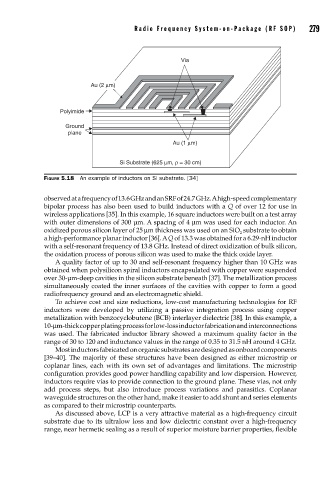
FIGURE 5.18 An example of inductors on Si substrate. [34]
observed at a frequency of 13.6 GHz and an SRF of 24.7 GHz. A high-speed complementary
bipolar process has also been used to build inductors with a Q of over 12 for use in
wireless applications [35]. In this example, 16 square inductors were built on a test array
with outer dimensions of 300 μm. A spacing of 4 μm was used for each inductor. An
oxidized porous silicon layer of 25 μm thickness was used on an SiO substrate to obtain
2
a high-performance planar inductor [36]. A Q of 13.3 was obtained for a 6.29-nH inductor
with a self-resonant frequency of 13.8 GHz. Instead of direct oxidization of bulk silicon,
the oxidation process of porous silicon was used to make the thick oxide layer.
A quality factor of up to 30 and self-resonant frequency higher than 10 GHz was
obtained when polysilicon spiral inductors encapsulated with copper were suspended
over 30-μm-deep cavities in the silicon substrate beneath [37]. The metallization process
simultaneously coated the inner surfaces of the cavities with copper to form a good
radiofrequency ground and an electromagnetic shield.
To achieve cost and size reductions, low-cost manufacturing technologies for RF
inductors were developed by utilizing a passive integration process using copper
metallization with benzocyclobutene (BCB) interlayer dielectric [38]. In this example, a
10-μm-thick copper plating process for low-loss inductor fabrication and interconnections
was used. The fabricated inductor library showed a maximum quality factor in the
range of 30 to 120 and inductance values in the range of 0.35 to 31.5 nH around 4 GHz.
Most inductors fabricated on organic substrates are designed as onboard components
[39–40]. The majority of these structures have been designed as either microstrip or
coplanar lines, each with its own set of advantages and limitations. The microstrip
configuration provides good power handling capability and low dispersion. However,
inductors require vias to provide connection to the ground plane. These vias, not only
add process steps, but also introduce process variations and parasitics. Coplanar
waveguide structures on the other hand, make it easier to add shunt and series elements
as compared to their microstrip counterparts.
As discussed above, LCP is a very attractive material as a high-frequency circuit
substrate due to its ultralow loss and low dielectric constant over a high-frequency
range, near hermetic sealing as a result of superior moisture barrier properties, flexible