
Page 367 - System on Package_ Miniaturization of the Entire System
P. 367
Integrated Chip-to-Chip Optoelectr onic SOP 339
6.5.2 Chip-to-Chip Optical Interconnects
Pioneering work in chip-to-chip optoelectronic integration on real-world, high-
performance computer motherboards was carried out by R. Chen in a university-industry
consortium [48–50] intended to improve the performance of mainframe computing at
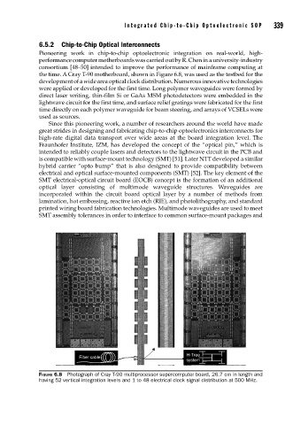
the time. A Cray T-90 motherboard, shown in Figure 6.8, was used as the testbed for the
development of a wide area optical clock distribution. Numerous innovative technologies
were applied or developed for the first time. Long polymer waveguides were formed by
direct laser writing, thin-film Si or GaAs MSM photodetectors were embedded in the
lightwave circuit for the first time, and surface relief gratings were fabricated for the first
time directly on each polymer waveguide for beam steering, and arrays of VCSELs were
used as sources.
Since this pioneering work, a number of researchers around the world have made
great strides in designing and fabricating chip-to-chip optoelectronics interconnects for
high-rate digital data transport over wide areas at the board integration level. The
Fraunhofer Institute, IZM, has developed the concept of the “optical pin,” which is
intended to reliably couple lasers and detectors to the lightwave circuit in the PCB and
is compatible with surface-mount technology (SMT) [51]. Later NTT developed a similar
hybrid carrier “opto bump” that is also designed to provide compatibility between
electrical and optical surface-mounted components (SMT) [52]. The key element of the
SMT electrical-optical circuit board (EOCB) concept is the formation of an additional
optical layer consisting of multimode waveguide structures. Waveguides are
incorporated within the circuit board optical layer by a number of methods from
lamination, hot embossing, reactive ion etch (RIE), and photolithography, and standard
printed wiring board fabrication technologies. Multimode waveguides are used to meet
SMT assembly tolerances in order to interface to common surface-mount packages and
H-Tree
Fiber cable
system
FIGURE 6.8 Photograph of Cray T-90 multiprocessor supercomputer board, 26.7 cm in length and
having 52 vertical integration levels and 1 to 48 electrical clock signal distribution at 500 MHz.